


 Dan’s Biz Bookshelf: Four Important Books You Need to Read (Not Just Say You Have)
 The Marketing Minute: Cracking the Code of Technical Marketing


The World's Fastest Nanoscale Photonics Switch
October 30, 2015 | Lomonosov Moscow State UniversityEstimated reading time: 3 minutes
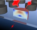
International team of researchers from Lomonosov Moscow State University and the Australian National University in Canberra created an ultrafast all-optical switch on silicon nanostructures. This device may become a platform for future computers and permit to transfer data at an ultrahigh speed.
This work belongs to the field of photonics, an optics discipline which appeared in the 1960s simultaneously with the invention of lasers. Photonics has the same goals as electronics does, but uses photons--the quanta of light--instead of electrons. The biggest advantage of using photons is the absence of interactions between them. As a consequence, photons address the data transmission problem better than electrons. This property can primarily be used for in computing where IPS (instructions per second) is the main attribute to be maximized. The typical scale of eletronic transistors--the basis of contemporary electronic devices--is less than 100 nanometers, wheres the typical scale of photonic transistors stays on the scale of several micrometers. Nanostructures that are able to compete with the electronic structures--for example, plasmonic nanoparticles--are characterized by low efficiency and significant losses. Therefore, coming up with a compact photonic switch was a very challenging task.
Three years ago several groups of researchers simultaneously discovered an important effect: they found out that silicon nanoparticles are exhibit strong resonances in the visible spectrum - the so-called magnetic dipole resonances. This type of resonance is characterized by strong localization of light waves on subwavelength scales, inside the nanoparticles. This effect turned out to be interesting to researches, but, according to Maxim Shcherbakov, the first author of the article published in Nano Letters, nobody thought that this discovery could create a basis for development of a compact and very rapid photonic switch.
Nanoparticles were fabricated in the Australian National University by e-beam lithography followed by plasma-phase etching. It was done by Alexander Shorokhov, who served an internship in the University as a part of Presidential scholarship for studying abroad. The samples were brought to Moscow, and all the experimental work was carried out at the Faculty of Physics of Lomonosov Moscow State University, in the Laboratory of Nanophotonics and Metamaterials.
"In our experimental research me and my colleague Polina Vabishchevich from the Faculty used a set of nonlinear optics methods that address femtosecond light-matter," explains Shcherbakov. "We used our femtosecond laser complex acquired as part of the MSU development program."
Eventually, researches developed a "device": a disc 250 nm in diameter that is capable of switching optical pulses at femtosecond rates (femtosecond is a one millionth of one billionth of a second). Switching speeds that fast will allow to create data transmission and processing devices that will work at tens and hundreds terabits per second. This can make possible downloading thousands of HD-movies in less than a second.
The operation of the all-optical switch created by MSU researchers is based on the interaction between two femtosecond pulses. The interaction becomes possible due to the magnetic resonance of the silicon nanostructures. If the pulses arrive at the nanostructure simultaneously, one of them interacts with the other and dampers it due to the effect of two-photon absorption. If there is a 100-fs delay between the two pulses, the interaction does not occur, and the second pulse goes through the nanostructure without changing.
"We were able to develop a structure with the undesirable free-carrier effects are suppressed," says Shcherbakov. "Free carriers (electrons and electron holes) place serious restrictions on the speed of signal conversion in the traditional integrated photonics. Our work represents an important step towards novel and efficient active photonic devices-- transistors, logic units, and others. Features of the technology implemented in our work will allow its use in silicon photonics. In the nearest future, we are going to test such nanoparticles in integrated circuits."
Share on:


Testimonial
"Advertising in PCB007 Magazine has been a great way to showcase our bare board testers to the right audience. The I-Connect007 team makes the process smooth and professional. We’re proud to be featured in such a trusted publication."
Klaus Koziol - atgSuggested Items
Closing the Loop on PCB Etching Waste
09/09/2025 | Shawn Stone, IECAs the PCB industry continues its push toward greener, more cost-efficient operations, Sigma Engineering’s Mecer System offers a comprehensive solution to two of the industry’s most persistent pain points: etchant consumption and rinse water waste. Designed as a modular, fully automated platform, the Mecer System regenerates spent copper etchants—both alkaline and acidic—and simultaneously recycles rinse water, transforming a traditionally linear chemical process into a closed-loop system.
The Chemical Connection: Through-glass Vias in Glass Substrates
06/24/2025 | Don Ball -- Column: The Chemical ConnectionThis month’s theme is vias and how best to ensure via quality and reliability. I don’t have much expertise in this process area or much to contribute that most of you don’t already know. However, I’ve recently become peripherally involved in a via technology that may be of more than academic interest to some of us. It entails putting vias in a material not usually associated with PCB manufacturing: through-glass vias (TGVs) in glass substrates.
In Pursuit of Perfection: Defect Reduction—May 2025 PCB007 Magazine Now Available
05/15/2025 | I-Connect007 Editorial TeamFor bare PCB board fabrication, defect reduction is a critical aspect of a company's bottom line profitability. In the May 2025 issue of PCB007 Magazine, we examine the imaging, etching, and plating processes, as well as product traceability on the shop floor, providing information and insight into how you can reduce your defects and increase yields.
DuPont to Showcase Advanced Semiconductor Wet Etching Innovations at the Surface Preparation and Cleaning Conference
05/13/2025 | DuPontDuPont announced that it will present its latest developments in semiconductor wet etching technologies at the upcoming Surface Preparation and Cleaning Conference (SPCC) in Chandler, Arizona, beginning May 20.
The Chemical Connection: Common Misconceptions in Wet Processing
04/28/2025 | Don Ball -- Column: The Chemical ConnectionInitially, I thought an April Fool’s column would be fun this month. I could highlight some of the crazier ideas and misconceptions I’ve witnessed over the years from potential customers and we could all have a good laugh. For example, there was a first-time buyer of a ferric chloride etcher (with no regeneration system) who was astonished to learn that he had to put fresh etchant in the system occasionally to maintain production.