-

- News
- Books
Featured Books
- design007 Magazine
Latest Issues
Current Issue
Rules of Thumb
This month, we delve into rules of thumb—which ones work, which ones should be avoided. Rules of thumb are everywhere, but there may be hundreds of rules of thumb for PCB design. How do we separate the wheat from the chaff, so to speak?

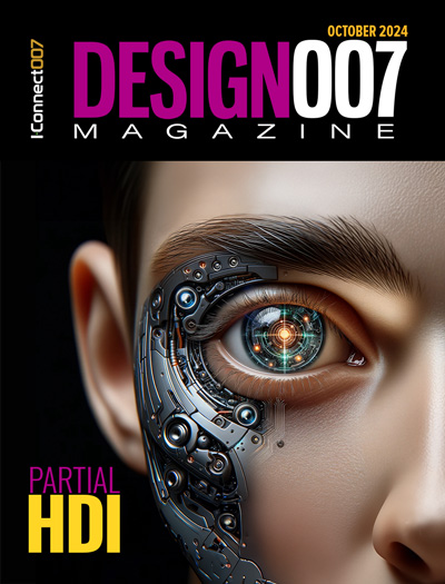
Partial HDI
Our expert contributors provide a complete, detailed view of partial HDI this month. Most experienced PCB designers can start using this approach right away, but you need to know these tips, tricks and techniques first.

Silicon to Systems: From Soup to Nuts
This month, we asked our expert contributors to weigh in on silicon to systems—what it means to PCB designers and design engineers, EDA companies, and the rest of the PCB supply chain... from soup to nuts.
- Articles
- Columns
Search Console
- Links
- Media kit
||| MENU - design007 Magazine
Accelerating the PCB Design Cycle
November 4, 2015 | Scott Miller, FreedomCAD ServicesEstimated reading time: 2 minutes
Mylar. Black tape. X-acto knives. Drafting tables. Ring lights.
These were the tools of the trade for the pioneers of printed circuit board design. Manually creating the large artwork that would then be photo-reduced to make the filmwork to image double-sided boards was truly an art form. The best designers were both neat and efficient. Somehow they avoided going home at night with their shirts or skirts covered with bits of tape stuck to them.
For those of you experienced designers, it’s incredible to see how far the art of PCB design has come over these 40+ years of evolution. CAD software has replaced Mylar, and computer screens have replaced lighted drafting tables. And now, it’s more science than art. PCB design now requires puzzle-solving skills on many levels to handle ever-increasing density and speed challenges.
The Need for Speed
By the mid-’90s, technologists were predicting that the use of conductive copper interconnections would need to be replaced with optics in order to address the increasing signal speeds. Year after year, the industry has found ways to increase the capabilities of copper interconnect to meet the escalating challenges. Some of these solutions were materials’ improvements such as high-speed laminates, smooth copper foil, and high-speed connectors. But many were based on PCB design strategies, including the use of back-drilling, reference planes, differential pairs, length matching, hole, pad and anti-pad shapes and sizes. Engineers and designers use many other strategies to maximize performance while minimizing cost.
One thing is clear: Designing printed circuit boards today is much more complicated and challenging than ever. Designing today’s leading-edge circuit boards requires that the designer:
- Has a strong knowledge of the capabilities of the CAD software.
- Understands PCB fabrication processes.
- Has a general knowledge of electronics and component functionality.
- Has a general knowledge of signal and power integrity.
- Understands PCB assembly processes.
- Understands industry specs.
In addition to all of these challenges, designers have to be efficient three-dimensional puzzles solvers because time-to-market is still a vitally important objective. After all, time is money.
So how do today’s designers balance the technical and timing demands? There isn’t one answer. It requires efficient use of the CAD tools, floor planning and effective communication with all parties involved.
Fortunately, Cadence Design Systems, Mentor Graphics, Altium and other PCB CAD software developers continue to make great strides at improving the capabilities of PCB layout tools. This has made it much faster to route differential pairs, create shapes or replicate circuits. And while they strive to make user interfaces logical and easy to use, many capabilities aren’t as obvious.
To read this entire article, which appeared in the October 2015 issue of The PCB Design Magazine, click here.
Suggested Items
Unlocking Advanced Circuitry Through Liquid Metal Ink
10/31/2024 | I-Connect007 Editorial TeamPCB UHDI technologist John Johnson of American Standard Circuits discusses the evolving landscape of electronics manufacturing and the critical role of innovation, specifically liquid metal ink technology, as an alternate process to traditional metallization in PCB fabrication to achieve ever finer features and tighter tolerances. The discussion highlights the benefits of reliability, efficiency, and yields as a tradeoff to any increased cost to run the process. As this technology becomes better understood and accepted, even sought out by customers and designers, John says there is a move toward mainstream incorporation.
Fresh PCB Concepts: The Critical Nature of Copper Thickness on PCBs
10/31/2024 | Team NCAB -- Column: Fresh PCB ConceptsPCBs are the backbone of modern electronics and the copper layers within these boards serve as the primary pathways for electrical signals. When designing and manufacturing PCBs, copper thickness is one of the most critical factors and significantly affects the board’s performance and durability. The IPC-6012F specification, the industry standard for the performance and qualification of rigid PCBs, sets clear guidelines on copper thickness to ensure reliability in different environments and applications.
Book Excerpt: The Printed Circuit Designer’s Guide to... DFM Essentials, Ch. 1
10/25/2024 | I-Connect007The guidelines offered in this book are based on both ASC recommendations and IPC standards with the understanding that some may require adjustment based on the material set, fabricator processes, and other design constraints. This chapter details high-frequency materials, copper foil types, metal core PCBs, and the benefits of embedded capacitance and resistor materials in multilayer PCBs.
The Cost-Benefit Analysis of Direct Metallization
10/21/2024 | Carmichael Gugliotti, MacDermid AlphaCarmichael Gugliotti of MacDermid Alpha discusses the innovative realm of direct metallization technology, its numerous applications, and significant advantages over traditional processes. Carmichael offers an in-depth look at how direct metallization, through developments such as Blackhole and Shadow, is revolutionizing PCB manufacturing by enhancing efficiency, sustainability, and cost-effectiveness. From its origins in the 1980s to its application in cutting-edge, high-density interconnects and its pivotal role in sustainability, this discussion sheds light on how direct metallization shapes the future of PCB manufacturing across various industries, including automotive, consumer electronics, and beyond.
Connect the Dots: Designing for Reality—Pattern Plating
10/16/2024 | Matt Stevenson -- Column: Connect the DotsIn the previous episode of I-Connect007’s On the Line with… podcast, we painted the picture of the outer layer imaging process. Now we are ready for pattern plating, where fabrication can get tricky. The board is now ready to receive the copper traces, pads, and other elements specified in the original CAD design. This article will lay out the pattern plating process and discuss constraints in the chemistries that must be properly managed to meet the customer's exacting manufacturing tolerances.


