


 Dan’s Biz Bookshelf: Four Important Books You Need to Read (Not Just Say You Have)
 The Marketing Minute: Cracking the Code of Technical Marketing


New Class of Materials for Organic Electronics
November 13, 2015 | Helmholtz-Zentrum Berlin für Materialien und EnergieEstimated reading time: 1 minute
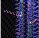
Polymeric carbon nitrides are organic compounds synthesised to form a yellow powder of a myriad of nanocrystals. The crystalline structure resembles that of graphite because the carbon nitride groups are chemically bound only in layers, while just weak Van der Waals forces provide cohesion between these layers. It was already known that light is able to create an electron-hole pair in this class of materials. So there have already been numerous attempts to employ polymeric carbon nitrides as cost-effective photocatalysts for solar-powered water splitting. However, the efficiency levels so far have remained comparatively low.
Light creates charge carriers
Now a team headed by Dr. Christoph Merschjann (HZB and Freie Universität Berlin) and Prof. Stefan Lochbrunner (University of Rostock) have for the first time precisely probed the processes occurring during light-induced charge separation. "The most interesting result has been that charges are basically only transported along one dimension during this process, perpendicular to the graphite-like layers", explains Merschjann. The light creates an electron-hole pair that subsequently migrates in opposing directions. Using femtosecond spectroscopy as well as other spectroscopic time-domain methods, the researchers were able to make the first quantitative mobility and lifetime measurements on the charge carriers. This revealed that the charge mobility attains values similar to those in conventional organic semiconductor materials. Moreover, the charge carriers are long-lived before recombining again.
New material for organic electronics
Polymeric carbon nitrides are not only non-toxic and cost-effective, they are also extremely durable because they are chemically very stable and can withstand temperatures of up to about 500 °C. Components made of these kinds of compounds might therefore be employed in environments that are unsuitable for today's organic electronics. Merschjann finds the prospect of growing these compounds on ordered substrates, such as graphene for example, especially interesting though. This is because graphene possesses extremely high in-plane conductivity, while carbon nitrides primarily conduct perpendicular to the sheets. "Carbon nitrides need not fear the competition with conventional organic semiconductor materials. On the contrary, completely new kinds of all-organic optoelectronic components might be built using their property of being essentially one-dimensional semiconductors", Merschjann hopes. He is currently working on making direct measurements of the charge carriers in a DFG-funded research project at Freie Universität Berlin.
Share on:


Testimonial
"Our marketing partnership with I-Connect007 is already delivering. Just a day after our press release went live, we received a direct inquiry about our updated products!"
Rachael Temple - AlltematedSuggested Items
Curing and Verification in PCB Shadow Areas
09/17/2025 | Doug Katze, DymaxDesign engineers know a simple truth that often complicates electronics manufacturing: Light doesn’t go around corners. In densely populated PCBs, adhesives and coatings often fail to fully cure in shadowed regions created by tall ICs, connectors, relays, and tight housings.
Marcy’s Musings: Advancing the Advanced Materials Discussion
09/17/2025 | Marcy LaRont -- Column: Marcy's MusingsAs the industry’s most trusted global source of original content about the electronics supply chain, we continually ask you about your concerns, what you care about, and what you most want to learn about. Your responses are insightful and valuable. Thank you for caring enough to provide useful feedback and engage in dialogue.
September 2025 PCB007 Magazine: The Future of Advanced Materials
09/16/2025 | I-Connect007 Editorial TeamMoore’s Law is no more, and the advanced material solutions being developed to grapple with this reality are surprising, stunning, and perhaps a bit daunting. Buckle up for a dive into advanced materials and a glimpse into the next chapters of electronics manufacturing.
I-Connect007 Launches Advanced Electronics Packaging Digest
09/15/2025 | I-Connect007I-Connect007 is pleased to announce the launch of Advanced Electronics Packaging Digest (AEPD), a new monthly digital newsletter dedicated to one of the most critical and rapidly evolving areas of electronics manufacturing: advanced packaging at the interconnect level.
Panasonic Industry will Double the Production Capacity of MEGTRON Multi-layer Circuit Board Materials Over the Next Five Years
09/15/2025 | Panasonic Industry Co., Ltd.Panasonic Industry Co., Ltd., a Panasonic Group company, announced plans for a major expansion of its global production capacity for MEGTRON multi-layer circuit board materials today. The company plans to double its production over the next five years to meet growing demand in the AI server and ICT infrastructure markets.