


 Dan’s Biz Bookshelf: Four Important Books You Need to Read (Not Just Say You Have)
 The Marketing Minute: Cracking the Code of Technical Marketing


Improving the Energy Efficiency of Topological Insulators
November 18, 2015 | FORSCHUNGSZENTRUM JUELICHEstimated reading time: 3 minutes
The overheating of computer chips is a major obstacle to the development of faster and more efficient computers and mobile phones. One promising remedy for this problem could be a class of materials first discovered just a few years ago: topological insulators, which conduct electricity with less resistance and heat generation than conventional materials. Research on these materials is still in its early stages. A team from Jülich and Aachen has now found a way to control the desired conducting properties of this type of material more precisely and reliably than ever before. The results have been published in the current edition of the journal Nature Communications (DOI: 10.1038/ncomms9816).
So-called "topological" materials have different physical properties on their surface than they do on their inside. Topological insulators are in effect insulators on the inside, but on their surfaces and edges they conduct electric currents almost as if they were running along railway tracks: faster, with less resistance and less heat production than with conventional materials. Additionally, the tracks act as a one-way street for electrons. The inherent angular momentum of the electrons - known as "spin" - determines in which direction the electrons can flow. This property is also useful for information processing and can pave the way for the development of new spintronic components.
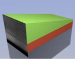
Researchers from the Peter Grünberg Institute and RWTH Aachen University have now shown how the conductivity and the energy requirements of these materials can be optimized. Put in highly simplified terms, their recipe for success is: stacking instead of mixing. Prof. Detlev Grützmacher of the Peter Grünberg Institute first came up with the crucially important idea: "Instead of alloying two different types of semi-conductors as usual, in order to obtain a topological insulator, we stacked both semiconductors on top of each other, atomic layer by atomic layer, placing this in turn on a silicon backing layer with the help of molecular beam epitaxy." Molecular beam epitaxy is an extremely precise method of producing thin crystalline layers, and is increasingly used not only in research but also in the industrial production of semiconductors.
In this way, the scientists were able to control the atomic construction with great precision, which they documented with the use of ultra high-resolution electron microscopy. "Achieving the perfect atomic composition of the topological insulators is vital for the electronic properties, and thus for energy efficiency, but the alloying process is difficult to monitor", explained Dr. Lukasz Plucinski from the Peter Grünberg Institute.
The researchers were able to discover exactly which layer thickness goes hand in hand with optimal conduction properties using the technology of angle-resolved photoemission spectroscopy. Here, samples are bombarded with photons to trigger the release of electrons from the material. Their energy and exit angle is measured, providing information about the energy and distribution of the electrons at the sample's surface.
In principle, topological insulators can also be controlled with the help of external electric fields in semiconductor alloys and other materials. Using the sandwich method that the scientists have developed together within the framework of the Jülich Aachen Research Alliance "Future Information Technology" (JARA FIT), such complex technological procedures are no longer necessary and in addition, the silicon substrate material makes it simpler to integrate in applications at later stages.
Scientists at the Virtual Institute for Topological Insulators (VITI), coordinated by the Peter Grünberg Institute in Jülich, are continuing to conduct basic research on further possible uses for the new materials. This could, for example, make it possible to prove the existence of novel, only theoretically predicted quantum phenomena, such as so called topological exciton condensates, formed by electron-hole pairs at the surfaces.
Share on:


Testimonial
"In a year when every marketing dollar mattered, I chose to keep I-Connect007 in our 2025 plan. Their commitment to high-quality, insightful content aligns with Koh Young’s values and helps readers navigate a changing industry. "
Brent Fischthal - Koh YoungSuggested Items
Curing and Verification in PCB Shadow Areas
09/17/2025 | Doug Katze, DymaxDesign engineers know a simple truth that often complicates electronics manufacturing: Light doesn’t go around corners. In densely populated PCBs, adhesives and coatings often fail to fully cure in shadowed regions created by tall ICs, connectors, relays, and tight housings.
Marcy’s Musings: Advancing the Advanced Materials Discussion
09/17/2025 | Marcy LaRont -- Column: Marcy's MusingsAs the industry’s most trusted global source of original content about the electronics supply chain, we continually ask you about your concerns, what you care about, and what you most want to learn about. Your responses are insightful and valuable. Thank you for caring enough to provide useful feedback and engage in dialogue.
September 2025 PCB007 Magazine: The Future of Advanced Materials
09/16/2025 | I-Connect007 Editorial TeamMoore’s Law is no more, and the advanced material solutions being developed to grapple with this reality are surprising, stunning, and perhaps a bit daunting. Buckle up for a dive into advanced materials and a glimpse into the next chapters of electronics manufacturing.
I-Connect007 Launches Advanced Electronics Packaging Digest
09/15/2025 | I-Connect007I-Connect007 is pleased to announce the launch of Advanced Electronics Packaging Digest (AEPD), a new monthly digital newsletter dedicated to one of the most critical and rapidly evolving areas of electronics manufacturing: advanced packaging at the interconnect level.
Panasonic Industry will Double the Production Capacity of MEGTRON Multi-layer Circuit Board Materials Over the Next Five Years
09/15/2025 | Panasonic Industry Co., Ltd.Panasonic Industry Co., Ltd., a Panasonic Group company, announced plans for a major expansion of its global production capacity for MEGTRON multi-layer circuit board materials today. The company plans to double its production over the next five years to meet growing demand in the AI server and ICT infrastructure markets.