


 Dan’s Biz Bookshelf: ‘Elevate: Push Beyond Your Limits'
 The Marketing Minute: The First Step to More Sales—Marketing
 It’s Only Common Sense: Customer Service Is Sales in Disguise


ESI Unveils Newest Addition to Its PCB Via Drilling Product Portfolio
December 7, 2015 | ESIEstimated reading time: 1 minute
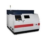
Electro Scientific Industries, Inc., an innovator of laser-based manufacturing solutions for the micromachining industry, today introduced its nViant™ laser processing system designed for High-Density Interconnect (HDI) applications. The nViant™ system expands ESI's portfolio of solutions for the Printed Circuit Board (PCB) industry. This portfolio already includes the industry-leading 5335 family of tools for flexible printed circuit via drilling as well as the CornerStone™ via drilling system for manufacturing high accuracy substrates used for integrated circuits.
A CO2 laser-based microvia drilling system, nViant™ combines excellent quality via formation with industry-leading accuracy on a robust platform that delivers high throughput at a competitive price point. The nViant™ system was designed and built for manufacturers of HDI boards, used in smartphones, wearables and other mobile devices. HDI components are also used in industrial and automotive markets.
High-volume manufacturing of HDI PCBs requires blind (BHV) and through-hole (LTH) via processing; these vias are typically created with laser drills, which offer fast, reliable, and cost-effective processing at a miniaturized scale. The nViant™ system enables HDI manufacturers to drill vias in a broad range of copper-clad base materials such as glass-woven reinforced epoxy resins (FR4) or other specialty materials. The nViant™ system joins ESI's long history of products targeted for the production floor and reinforces ESI's focus and experience on speed, quality and accuracy.
"nViant™ leverages our expertise in laser processing and our proven track record of success in laser-based systems—especially in the flexible PCB manufacturing segment, where ESI is the clear market leader—and applies it to the HDI manufacturing segment," said Chris Ryder, Director of HDI Product Management at ESI. "The nViant™ system delivers a compelling solution for HDI PCB manufacturers. It's engineered to provide great reliability at high-quality output with the industry's lowest cost of ownership, and is backed by ESI's professional service and support organization with local offices throughout the world."
For PCB manufacturers of HDI boards, CO2 laser processing is the optimal choice for overall lower cost of ownership. ESI's nViant™ system extends this advantage with robust platform construction that allows for 24/7 operation. Support is provided through ESI's professional service organization.
The launch of nViant™ is taking place in conjunction with the 2015 International Printed Circuit & APEX South China Fair (2015 HKPCA & IPC Show) December 2-4 at the Shenzhen Convention and Exhibition Center in Shenzhen, China.
Share on:


Suggested Items
I-Connect007 Editor’s Choice: Five Must-Reads for the Week
07/18/2025 | Nolan Johnson, I-Connect007It may be the middle of the summer, but the news doesn’t quit, and there’s plenty to talk about this week, whether you’re talking technical or on a global scale. When I have to choose six items instead of my regular five, you know it’s good. I start by highlighting my interview with Martyn Gaudion on his latest book, share some concerning tariff news, follow that up with some promising (and not-so-promising) investments, and feature a paper from last January’s inaugural Pan-European Design Conference.
Elephantech Launches World’s Smallest-Class Copper Nanofiller
07/17/2025 | ElephantechJapanese deep-tech startup Elephantech has launched its cutting-edge 15 nm class copper nanofiller – the smallest class available globally. This breakthrough makes Elephantech one of the first companies in the world to provide such advanced material for commercial use.
Copper Price Surge Raises Alarms for Electronics
07/15/2025 | Global Electronics Association Advocacy and Government Relations TeamThe copper market is experiencing major turbulence in the wake of U.S. President Donald Trump’s announcement of a 50% tariff on imported copper effective Aug. 1. Recent news reports, including from the New York Times, sent U.S. copper futures soaring to record highs, climbing nearly 13% in a single day as manufacturers braced for supply shocks and surging costs.
I-Connect007 Editor’s Choice: Five Must-Reads for the Week
07/11/2025 | Andy Shaughnessy, Design007 MagazineThis week, we have quite a variety of news items and articles for you. News continues to stream out of Washington, D.C., with tariffs rearing their controversial head again. Because these tariffs are targeted at overseas copper manufacturers, this news has a direct effect on our industry.I-Connect007 Editor’s Choice: Five Must-Reads for the Week
Digital Twin Concept in Copper Electroplating Process Performance
07/11/2025 | Aga Franczak, Robrecht Belis, Elsyca N.V.PCB manufacturing involves transforming a design into a physical board while meeting specific requirements. Understanding these design specifications is crucial, as they directly impact the PCB's fabrication process, performance, and yield rate. One key design specification is copper thieving—the addition of “dummy” pads across the surface that are plated along with the features designed on the outer layers. The purpose of the process is to provide a uniform distribution of copper across the outer layers to make the plating current density and plating in the holes more uniform.