


 Dan’s Biz Bookshelf: Four Important Books You Need to Read (Not Just Say You Have)
 The Marketing Minute: Cracking the Code of Technical Marketing


NIST Adds to Quantum Computing Toolkit with Mixed-atom Logic Operations
December 16, 2015 | NISTEstimated reading time: 2 minutes
Physicists at the National Institute of Standards and Technology (NIST) have added to their collection of ingredients for future quantum computers by performing logic operations--basic computing steps--with two atoms of different elements. This hybrid design could be an advantage in large computers and networks based on quantum physics.
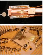
The NIST experiment, described in the Dec. 17 issue of Nature,* manipulated one magnesium and one beryllium ion (charged atom) confined in a custom trap (see photo). The scientists used two sets of laser beams to entangle the two ions--establishing a special quantum link between their properties--and to perform two types of logic operations, a controlled NOT (CNOT) gate and a SWAP gate. The same issue of Nature describes similar work with two forms of calcium ions performed at the University of Oxford.
"Hybrid quantum computers allow the unique advantages of different types of quantum systems to be exploited together in a single platform," said lead author Ting Rei Tan. "Many research groups are pursuing this general approach. Each ion species is unique, and certain ones are better suited for certain tasks such as memory storage, while others are more suited to provide interconnects for data transfer between remote systems."
Gates are used to build circuits or programs. As in classical computing, a quantum bit (qubit) can have a value of 0 or 1. But unlike classical bits, a qubit can also be in a "superposition" of both 0 and 1 values at the same time. In the NIST experiment, the qubits are based on the ions' spin directions (spin up is 1 and spin down is 0). A CNOT gate flips the second (target) qubit if the first (control) qubit is a 1; if it is a 0, the target bit is unchanged. If the control qubit is in a superposition, the ions become entangled. A SWAP gate interchanges the qubit states, including superpositions.
The two types of ions vary in their response to light, so lasers can be tuned to manipulate one without disturbing the other. This minimizes interference. But getting the whole setup to operate coherently was a challenge. The researchers developed a technique to track and stabilize the laser beam phases, that is, the exact positions of the undulating light waves.
Page 1 of 2
Share on:


Testimonial
"In a year when every marketing dollar mattered, I chose to keep I-Connect007 in our 2025 plan. Their commitment to high-quality, insightful content aligns with Koh Young’s values and helps readers navigate a changing industry. "
Brent Fischthal - Koh YoungSuggested Items
Weaning the U.S. Military Off a Tablet Supply Chain That Leads to China
09/08/2025 | Jim Will, USPAETablet computers are essential to how our military fights, moves and sustains, but these devices are built on a fragile global supply chain with strong ties to China. Building domestic manufacturing to eliminate this vulnerability is feasible if we tap into the information and capabilities that already exist and create strong demand for tablets produced by trusted and assured sources.
Fresh PCB Concepts: Designing for Success at the Rigid-flex Transition Area
08/28/2025 | Team NCAB -- Column: Fresh PCB ConceptsRigid-flex PCBs come in all shapes and sizes. Manufacturers typically use fire-retardant, grade 4 (FR-4) materials in the rigid section and flexible polyimide materials in the flex region. Because of the small size, some rigid-flex PCBs, like those for hearing aid devices, are among the most challenging to manufacture. However, regardless of its size, we should not neglect the transition area between the rigid and flexible material.
Semiconductors Get Magnetic Boost with New Method from UCLA Researchers
07/31/2025 | UCLA NewsroomA new method for combining magnetic elements with semiconductors — which are vital materials for computers and other electronic devices — was unveiled by a research team led by the California NanoSystems Institute at UCLA.
Japan’s OHISAMA Project Aims to Beam Solar Power from Space This Year
07/14/2025 | I-Connect007 Editorial TeamJapan could be on the cusp of making history with its OHISAMA project in its quest to become the first country to transmit solar power from space to Earth, The Volt reported.
The Big Picture: Our Big ‘Why’ in the Age of AI
06/25/2025 | Mehul Davé -- Column: The Big PictureWith advanced technology, Tesla, Google, Microsoft, and OpenAI can quickly transform life as we know it. Several notable artificial intelligence (AI) studies, including the 2024 McKinsey Global Survey on AI, have offered insights into AI’s adoption, impact, and trajectory. The McKinsey study revealed that AI adoption continues to grow, with 50% of respondents reporting using AI in at least one business area.