


 Dan’s Biz Bookshelf: Four Important Books You Need to Read (Not Just Say You Have)
 The Marketing Minute: Cracking the Code of Technical Marketing


Nanowalls for Smartphones
January 7, 2016 | ETH ZurichEstimated reading time: 3 minutes
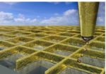
Researchers at ETH Zurich have manufactured transparent electrodes for use in touchscreens using a novel nanoprinting process. The new electrodes are some of the most transparent and conductive that have ever been developed.
From smartphones to the operating interfaces of ticket machines and cash dispensers, every touchscreen we use requires transparent electrodes: The devices’ glass surface is coated with a barely visible pattern made of conductive material. It is because of this that the devices recognise whether and where exactly a finger is touching the surface.
Researchers under the direction of Dimos Poulikakos, Professor of Thermodynamics, have now used 3D print technology to create a new type of transparent electrode, which takes the form of a grid made of gold or silver “nanowalls” on a glass surface. The walls are so thin that they can hardly be seen with the naked eye. It is the first time that scientists have created nanowalls like these using 3D printing. The new electrodes have a higher conductivity and are more transparent than those made of indium tin oxide, the standard material used in smartphones and tablets today. This is a clear advantage: The more transparent the electrodes, the better the screen quality. And the more conductive they are, the more quickly and precisely the touchscreen will work.
“Indium tin oxide is used because the material has a relatively high degree of transparency and the production of thin layers has been well researched, but it is only moderately conductive,” says Patrik Rohner, a PhD student in Poulikakos’ team. In order to produce more conductive electrodes, the ETH researchers opted for gold and silver, which conduct electricity much better. But because these metals are not transparent, the scientists had to make use of the third dimension. ETH professor Poulikakos explains: “If you want to achieve both high conductivity and transparency in wires made from these metals, you have a conflict of objectives. As the cross-sectional area of gold and silver wires grows, the conductivity increases, but the grid’s transparency decreases.”
The solution was to use metal walls only 80 to 500 nanometres thick, which are almost invisible when viewed from above. Because they are two to four times taller than they are wide, the cross-sectional area, and thus the conductivity, is sufficiently high.
Page 1 of 2
Share on:


Testimonial
"The I-Connect007 team is outstanding—kind, responsive, and a true marketing partner. Their design team created fresh, eye-catching ads, and their editorial support polished our content to let our brand shine. Thank you all! "
Sweeney Ng - CEE PCBSuggested Items
Meet the Author Podcast: Martyn Gaudion Unpacks the Secrets of High-Speed PCB Design
07/16/2025 | I-Connect007In this special Meet the Author episode of the On the Line with… podcast, Nolan Johnson sits down with Martyn Gaudion, signal integrity expert, managing director of Polar Instruments, and three-time author in I-Connect007’s popular The Printed Circuit Designer’s Guide to... series.
Intervala Hosts Employee Car and Motorcycle Show, Benefit Nonprofits
08/27/2024 | IntervalaIntervala hosted an employee car and motorcycle show, aptly named the Vala-Cruise and it was a roaring success! Employees had the chance to show off their prized wheels, and it was incredible to see the variety and passion on display.
KIC Honored with IPC Recognition for 25 Years of Membership and Contributions to Electronics Manufacturing Industry
06/24/2024 | KICKIC, a renowned pioneer in thermal process and temperature measurement solutions for electronics manufacturing, is proud to announce that it has been recognized by IPC for 25 years of membership and significant contributions to electronics manufacturing.
Boeing Starliner Spacecraft Completes Successful Crewed Docking with International Space Station
06/07/2024 | BoeingNASA astronauts Barry "Butch" Wilmore and Sunita "Suni" Williams successfully docked Boeing's Starliner spacecraft to the International Space Station (ISS), about 26 hours after launching from Cape Canaveral Space Force Station.
KIC’s Miles Moreau to Present Profiling Basics and Best Practices at SMTA Wisconsin Chapter PCBA Profile Workshop
01/25/2024 | KICKIC, a renowned pioneer in thermal process and temperature measurement solutions for electronics manufacturing, announces that Miles Moreau, General Manager, will be a featured speaker at the SMTA Wisconsin Chapter In-Person PCBA Profile Workshop.