


 Dan’s Biz Bookshelf: Four Important Books You Need to Read (Not Just Say You Have)
 The Marketing Minute: Cracking the Code of Technical Marketing


Visualizing Atoms of Perovskite Crystals
January 10, 2016 | Okinawa Institute of Science and Technology (OIST) Graduate UniversityEstimated reading time: 2 minutes
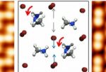
Organic-inorganic perovskite materials are key components of the new generation of solar cells. Understanding properties of these materials is important for improving lifetime and quality of solar cells. Researchers from the Energy Materials and Surface Sciences (EMSS) Unit, led by Prof. Yabing Qi, at the Okinawa Institute of Science and Technology Graduate University (OIST) in collaboration with Prof. Youyong Li's group from Soochow University (China) and Prof. Nam-Gyu Park's group from Sungkyunkwan University (Korea) report in the Journal of the American Chemical Society the first atomic resolution study of organic-inorganic perovskite.
Perovskites are a class of materials with the general chemical formula ABX3. A and B are positive ions bound by negative ions X. Organic-inorganic perovskites used in solar cells are usually methylammonium lead halides (CH3NH3PbX3, where X is bromine, iodine, or chlorine). The OIST scientists used a single crystal of methylammonium lead bromide (CH3NH3PbBr3) to create topographic images of its surface with a scanning tunneling microscope.
This microscope uses a conducting tip that moves across the surface in a manner very similar to a finger moving across a Braille sign. While the bumps in Braille signs are a few millimetres apart, the microscope detects bumps that are more than million times smaller -- atoms and molecules. This is achieved by the quantum tunneling effect -- the ability of an electron to pass through a barrier. The probability of an electron passing between the material surface and the tip depends on the distance between the two. The resulting atomic-resolution topographic images reveal positions and orientations of atoms and molecules, and also provide a detailed look at structural defects in the surface.
"At room temperature atoms and molecules are quite mobile, so we decided to freeze the crystal to almost absolute zero (-269ºC) to get a good picture of its atomic structure," says Dr Robin Ohmann, a member of the EMSS Unit and the first author of the paper. The crystal was cut and studied in a vacuum to avoid contamination of the surface. Dr Ohmann's colleagues from Soochow University calculated atomic structures using principles of quantum physics and then compared them with scanning tunneling microscopy data.
Page 1 of 2
Share on:


Testimonial
"Advertising in PCB007 Magazine has been a great way to showcase our bare board testers to the right audience. The I-Connect007 team makes the process smooth and professional. We’re proud to be featured in such a trusted publication."
Klaus Koziol - atgSuggested Items
Curing and Verification in PCB Shadow Areas
09/17/2025 | Doug Katze, DymaxDesign engineers know a simple truth that often complicates electronics manufacturing: Light doesn’t go around corners. In densely populated PCBs, adhesives and coatings often fail to fully cure in shadowed regions created by tall ICs, connectors, relays, and tight housings.
Marcy’s Musings: Advancing the Advanced Materials Discussion
09/17/2025 | Marcy LaRont -- Column: Marcy's MusingsAs the industry’s most trusted global source of original content about the electronics supply chain, we continually ask you about your concerns, what you care about, and what you most want to learn about. Your responses are insightful and valuable. Thank you for caring enough to provide useful feedback and engage in dialogue.
September 2025 PCB007 Magazine: The Future of Advanced Materials
09/16/2025 | I-Connect007 Editorial TeamMoore’s Law is no more, and the advanced material solutions being developed to grapple with this reality are surprising, stunning, and perhaps a bit daunting. Buckle up for a dive into advanced materials and a glimpse into the next chapters of electronics manufacturing.
I-Connect007 Launches Advanced Electronics Packaging Digest
09/15/2025 | I-Connect007I-Connect007 is pleased to announce the launch of Advanced Electronics Packaging Digest (AEPD), a new monthly digital newsletter dedicated to one of the most critical and rapidly evolving areas of electronics manufacturing: advanced packaging at the interconnect level.
Panasonic Industry will Double the Production Capacity of MEGTRON Multi-layer Circuit Board Materials Over the Next Five Years
09/15/2025 | Panasonic Industry Co., Ltd.Panasonic Industry Co., Ltd., a Panasonic Group company, announced plans for a major expansion of its global production capacity for MEGTRON multi-layer circuit board materials today. The company plans to double its production over the next five years to meet growing demand in the AI server and ICT infrastructure markets.