


 SMT Perspectives & Prospects: Artificial Intelligence Part 6: Data Module 1
 Standard of Excellence: Overcoming Service Failures—The Art of the Apology
 Nolan’s Notes: Tariffs, Technologies, and Optimization


Mek Introduces ISO-Spector, Inline 3D Topographical & Imaging AOI
January 12, 2016 | Mek (Marantz Electronics)Estimated reading time: 1 minute
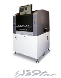
The completely new ISO-Spector from leading AOI manufacturer Mek (Marantz Electronics), is an AOI system of 'true measurement' for the full across-the-board inspection of components and solder joints.
Unlike other methods of height measurement, ISO-Spector technology enables inspection of heights up to 30 mm (1.2"), and is practically immune to vibrations from nearby placement machines which might otherwise cause blurry images and therefore inaccurate and non-repeatable results during production. It is able to inspect the world’s smallest chip size of 008004 (50% of 01005") and features a full profile simultaneous 2D and 3D inspection while maintaining high inspection speed using patented sensor technology.
The image capturing sensor has a massive 12 Mega Pixel resolution with optical fibre interface. The ISO-Spector enables accurate height measurement by using front & rear, close to vertical, high energy, high-end violet lasers. These lasers, combined with proprietary algorithms, result in the minimization of blind spots (shadow) and the effect of reflecting objects. Warped PCB’s up to 4 mm (160 mils) are compensated for on the fly by the Z-axis and complex compensation algorithms.
Unique for these type of inspection systems, the ISO-Spector can be programmed and debugged offline using the offline programming and debugging stations.
The 3D AOI system is ergonomically designed and operated via a full touch screen.
ISO-Spector integrates fully with the FIBER system for classification, repair, traceability and SPC.
About Mek (Marantz Electronics Ltd)
A former division of Marantz well known for its high quality Audio/Video products, Mek Japan (Marantz Electronics Kabushiki Kaisha), developed its first AOI system in 1994. Developed to inspect PCB assemblies for correct component placement and soldering, the company’s original AOI system was designed for use in Marantz factories. Proving to be a highly successful, cost-effective alternative to traditional human inspection, Mek developed its first generation commercial system in 1996. With a steadily growing installed base, MEK Japan and its European/American headquarters, Mek, have sold over 5000 units worldwide to date. Now well established as a leading force in AOI technologies, the company also manufactures a 5D post-print SPI system which combines 3D and 2D image processing methodologies to deliver unprecedented defect detection. At the beginning of March 2014 the company opened US offices in Las Vegas.
Share on:


Testimonial
"Our marketing partnership with I-Connect007 is already delivering. Just a day after our press release went live, we received a direct inquiry about our updated products!"
Rachael Temple - AlltematedSuggested Items
Indium to Showcase High-Reliability Solder and Flux-Cored Wire Solutions at SMTA International
10/09/2025 | Indium CorporationAs one of the leading materials providers in the electronics industry, Indium Corporation® will feature its innovative, high-reliability solder and flux-cored wire products at SMTA International (SMTAI), to be held October 19-23 in Rosemont, Illinois.
‘Create your Connections’ – Rehm at productronica 2025 in Munich
10/08/2025 | Rehm Thermal SystemsThe electronics industry is undergoing dynamic transformation: smart production lines, sustainability, artificial intelligence, and sensor technologies dominate current discussions.
Amplifying Innovation: New Podcast Series Spotlights Electronics Industry Leaders
10/08/2025 | I-Connect007In the debut episode, “Building Reliability: KOKI’s Approach to Solder Joint Challenges,” host Marcy LaRont speaks with Shantanu Joshi, Head of Customer Solutions and Operational Excellence at KOKI Solder America. They explore how advanced materials, such as crack-free fluxes and zero-flux-residue solder pastes, are addressing issues like voiding, heat dissipation, and solder joint reliability in demanding applications, where failure can result in costly repairs or even catastrophic loss.
SASinno Americas Introduces the Ultra Series
10/07/2025 | SASinno AmericasSASinno Americas has introduced the new Ultra Series, the latest generation of offline selective soldering systems. Available in two models—the Ultra-i1 and Ultra-i2—the new series is designed to meet the needs of manufacturers running small to medium batch sizes, multiple product types, and frequent line changes, while maintaining exceptional precision and process control.
Elmotec by E-Tronix to Showcase SolderSmart® TOP Robotic Soldering at The Assembly Show 2025
10/06/2025 | ELMOTECE-tronix, a Stromberg Company, is pleased to announce its participation at The Assembly Show 2025 in Rosemont, IL, October 21st through 23rd. Exhibiting under Elmotec by E-Tronix, Booth #448, the team will highlight the SolderSmart® TOP robotic soldering system, featuring live demonstrations throughout the show.