-
- News
- Books
Featured Books
- pcb007 Magazine
Latest Issues
Current IssueInventing the Future with SEL
Two years after launching its state-of-the-art PCB facility, SEL shares lessons in vision, execution, and innovation, plus insights from industry icons and technology leaders shaping the future of PCB fabrication.
Sales: From Pitch to PO
From the first cold call to finally receiving that first purchase order, the July PCB007 Magazine breaks down some critical parts of the sales stack. To up your sales game, read on!
The Hole Truth: Via Integrity in an HDI World
From the drilled hole to registration across multiple sequential lamination cycles, to the quality of your copper plating, via reliability in an HDI world is becoming an ever-greater challenge. This month we look at “The Hole Truth,” from creating the “perfect” via to how you can assure via quality and reliability, the first time, every time.
- Articles
- Columns
- Links
- Media kit
||| MENU - pcb007 Magazine
Ventec to Unveil New 'tec-speed' Brand for High Speed/Low Loss Materials at DesignCon 2016
January 13, 2016 | Ventec International GroupEstimated reading time: 2 minutes
Ventec International Group, a world leader in the production of polyimide & high reliability epoxy laminates and prepregs, will exhibit in Booth 118 at DesignCon 2016 (January 20th to 21st 2016, Santa Clara, CA, USA) where the company will launch a new brand identity, tec-speed, for its high speed/low loss product line. With the launch, Ventec will unveil a new logo, marketing collateral and technical specifications.
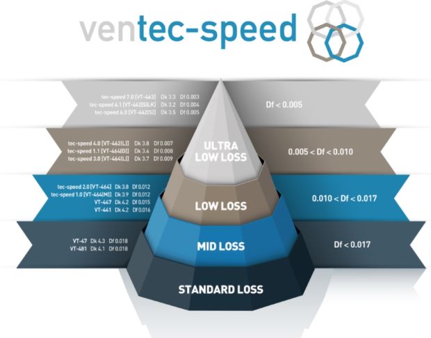
The creation of the brand name 'tec-speed' is a move to unite Ventec's high speed/low loss product portfolio and better position the range under a single identity, connecting the products through a clear and cohesive visual presentation.
Martin Cotton, Director OEM Technology, commented: “The tec-speed brand now unites one of the most comprehensive range of products in high speed/low loss PCB material technology. Every tec-speed product provides technological innovation, high performance and quality to customers to perfectly meet their needs.”
Ventec International Group’s COO USA & EUROPE, Mark Goodwin added: “With the growing demand for high reliability and high speed computing & storage applications, and a pipeline of new innovative additions to our range, the timing is right to give our product line a clear identity. More than that, our unique approach to supply chain ownership, with a manufacturing and distribution network that covers the relevant markets globally, ensures fast delivery of quality materials”.
A selection of products will be highlighted at the show, including:
tec-speed 6.1 (Dk 3.2, Df 0.004 RC 50%) - Ultra-Low Loss High Tg material available with all copper styles, including HVLP. Uses Low Dk spread glass to improve Skew and Jitter. Applications include Telecom, Router, Servers etc. Specifically, backplane and daughter card designs where good Signal Integrity is essential. This material has excellent Thermal properties.
tec-speed 4.0 (Dk 3.8, Df 0.007) - Low-Loss High Tg material available with all copper styles, including HVLP. Applications focus on High Frequency & High Speed designs, Automotive and Satellite communication, Navigation, GPS, etc. are typical applications. This material has excellent thermal properties.
tec-speed 1.0 (Dk 3.9, Df 0.012 @ 10GHz RC75%) - Mid-Loss Mid Tg Halogen Free material available with all copper styles. Applications include hand-held products, specifically those that require high frequency high speed materials. This material has excellent thermal properties.
For more information about Ventec’s solutions and the company’s wide variety of products, please visit www.venteclaminates.com or download to the Ventec APP.
About Ventec International
With volume manufacturing facilities and HQ in Suzhou China, Ventec International specializes in advanced copper clad glass reinforced and metal backed substrates for the PCB industry. With distribution locations and quick-turn CCL manufacturing sites in both the US and Europe, Ventec International is a premier supplier to the Global PCB industry. For more information, visit www.venteclaminates.com, www.ventec-usa.com or www.ventec-europe.com.
Testimonial
"In a year when every marketing dollar mattered, I chose to keep I-Connect007 in our 2025 plan. Their commitment to high-quality, insightful content aligns with Koh Young’s values and helps readers navigate a changing industry. "
Brent Fischthal - Koh YoungSuggested Items
Trouble in Your Tank: Implementing Direct Metallization in Advanced Substrate Packaging
09/15/2025 | Michael Carano -- Column: Trouble in Your TankDirect metallization systems based on conductive graphite are gaining popularity throughout the world. The environmental and productivity gains achievable with this process are outstanding. Direct metallization reduces the costs of compliance, waste treatment, and legal issues related to chemical exposure. A graphite-based direct plate system has been devised to address these needs.
Closing the Loop on PCB Etching Waste
09/09/2025 | Shawn Stone, IECAs the PCB industry continues its push toward greener, more cost-efficient operations, Sigma Engineering’s Mecer System offers a comprehensive solution to two of the industry’s most persistent pain points: etchant consumption and rinse water waste. Designed as a modular, fully automated platform, the Mecer System regenerates spent copper etchants—both alkaline and acidic—and simultaneously recycles rinse water, transforming a traditionally linear chemical process into a closed-loop system.
Driving Innovation: Depth Routing Processes—Achieving Unparalleled Precision in Complex PCBs
09/08/2025 | Kurt Palmer -- Column: Driving InnovationIn PCB manufacturing, the demand for increasingly complex and miniaturized designs continually pushes the boundaries of traditional fabrication methods, including depth routing. Success in these applications demands not only on robust machinery but also sophisticated control functions. PCB manufacturers rely on advanced machine features and process methodologies to meet their precise depth routing goals. Here, I’ll explore some crucial functions that empower manufacturers to master complex depth routing challenges.
Trouble in Your Tank: Minimizing Small-via Defects for High-reliability PCBs
08/27/2025 | Michael Carano -- Column: Trouble in Your TankTo quote the comedian Stephen Wright, “If at first you don’t succeed, then skydiving is not for you.” That can be the battle cry when you find that only small-diameter vias are exhibiting voids. Why are small holes more prone to voids than larger vias when processed through electroless copper? There are several reasons.
The Government Circuit: Navigating New Trade Headwinds and New Partnerships
08/25/2025 | Chris Mitchell -- Column: The Government CircuitAs global trade winds continue to howl, the electronics manufacturing industry finds itself at a critical juncture. After months of warnings, the U.S. Government has implemented a broad array of tariff increases, with fresh duties hitting copper-based products, semiconductors, and imports from many nations. On the positive side, tentative trade agreements with Europe, China, Japan, and other nations are providing at least some clarity and counterbalance.