


 Dan’s Biz Bookshelf: Four Important Books You Need to Read (Not Just Say You Have)
 The Marketing Minute: Cracking the Code of Technical Marketing


Nanodevice, Build Thyself
January 15, 2016 | Alpha GalileoEstimated reading time: 3 minutes
Researchers in Germany studied how a multitude of electronic interactions govern the encounter between a molecule called porphine and copper and silver surfaces – information that could one day be harnessed to make molecular building blocks self-assemble into nanodevices.
As we continue to shrink electronic components, top-down manufacturing methods begin to approach a physical limit at the nanoscale. Rather than continue to chip away at this limit, one solution of interest involves using the bottom-up self-assembly of molecular building blocks to build nanoscale devices.
Successful self-assembly is an elaborately choreographed dance, in which the attractive and repulsive forces within molecules, between each molecule and its neighbors, and between molecules and the surface that supports them, have to all be taken into account. To better understand the self-assembly process, researchers at the Technical University of Munich have characterized the contributions of all interaction components, such as covalent bonding and van der Waals interactions between molecules and between molecules and a surface.
“In an ideal case, the smallest possible device has the size of a single atom or molecule,” said Katharina Diller, who worked as a postdoctoral researcher in the group of Karsten Reuter at the Technical University of Munich. Reuter and his colleagues present their work this week in The Journal of Chemical Physics, from AIP Publishing.
One such example is a single-porphyrin switch, which occupies a surface area of only one square nanometer. The porphine molecule, which was the object of this study, is even smaller than this. Porphyrins are a group of ringed chemical compounds which notably include heme – responsible for transporting oxygen and carbon dioxide in the bloodstream – and chlorophyll. In synthetically-derived applications, porphyrins are studied for their potential uses as sensors, light-sensitive dyes in organic solar cells, and molecular magnets.
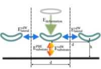
Schematic depiction of different energy terms contributing to the adsorption energy, and charge density difference of 2H-P after adsorption onto Cu(111) at 12.8 Angstrom separation. Image Credit: M. Müller/TU Munich
Page 1 of 2
Share on:


Testimonial
"Advertising in PCB007 Magazine has been a great way to showcase our bare board testers to the right audience. The I-Connect007 team makes the process smooth and professional. We’re proud to be featured in such a trusted publication."
Klaus Koziol - atgSuggested Items
Electrodeposited Copper Foils Market to Grow by $11.7 Billion Over 2025-2032
09/18/2025 | Globe NewswireThe global electrodeposited copper foils market is poised for dynamic growth, driven by the rising adoption in advanced electronics and renewable energy storage solutions.
MacDermid Alpha Showcases Advanced Interconnect Solutions at PCIM Asia 2025
09/18/2025 | MacDermid Alpha Electronics SolutionsMacDermid Alpha Electronic Solutions, a global leader in materials for power electronics and semiconductor assembly, will showcase its latest interconnect innovations in electronic interconnect materials at PCIM Asia 2025, held from September 24 to 26 at the Shanghai New International Expo Centre, Booth N5-E30
Trouble in Your Tank: Implementing Direct Metallization in Advanced Substrate Packaging
09/15/2025 | Michael Carano -- Column: Trouble in Your TankDirect metallization systems based on conductive graphite are gaining popularity throughout the world. The environmental and productivity gains achievable with this process are outstanding. Direct metallization reduces the costs of compliance, waste treatment, and legal issues related to chemical exposure. A graphite-based direct plate system has been devised to address these needs.
Closing the Loop on PCB Etching Waste
09/09/2025 | Shawn Stone, IECAs the PCB industry continues its push toward greener, more cost-efficient operations, Sigma Engineering’s Mecer System offers a comprehensive solution to two of the industry’s most persistent pain points: etchant consumption and rinse water waste. Designed as a modular, fully automated platform, the Mecer System regenerates spent copper etchants—both alkaline and acidic—and simultaneously recycles rinse water, transforming a traditionally linear chemical process into a closed-loop system.
Driving Innovation: Depth Routing Processes—Achieving Unparalleled Precision in Complex PCBs
09/08/2025 | Kurt Palmer -- Column: Driving InnovationIn PCB manufacturing, the demand for increasingly complex and miniaturized designs continually pushes the boundaries of traditional fabrication methods, including depth routing. Success in these applications demands not only on robust machinery but also sophisticated control functions. PCB manufacturers rely on advanced machine features and process methodologies to meet their precise depth routing goals. Here, I’ll explore some crucial functions that empower manufacturers to master complex depth routing challenges.