


 Dan’s Biz Bookshelf: Four Important Books You Need to Read (Not Just Say You Have)
 The Marketing Minute: Cracking the Code of Technical Marketing


Tiny Electronic Implants Monitor Brain Injury, Then Melt Away
January 20, 2016 | University of Illinois at Urbana-ChampaignEstimated reading time: 3 minutes
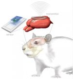
A new class of small, thin electronic sensors can monitor temperature and pressure within the skull - crucial health parameters after a brain injury or surgery - then melt away when they are no longer needed, eliminating the need for additional surgery to remove the monitors and reducing the risk of infection and hemorrhage.
Similar sensors can be adapted for postoperative monitoring in other body systems as well, the researchers say. Led by John A. Rogers, a professor of materials science and engineering at the University of Illinois at Urbana-Champaign, and Wilson Ray, a professor of neurological surgery at the Washington University School of Medicine in St. Louis, the researchers publish their work in the journal Nature on January 18.
"This is a new class of electronic biomedical implants," said Rogers, who directs the Frederick Seitz Materials Research Laboratory at Illinois. "These kinds of systems have potential across a range of clinical practices, where therapeutic or monitoring devices are implanted or ingested, perform a sophisticated function, and then resorb harmlessly into the body after their function is no longer necessary."
After a traumatic brain injury or brain surgery, it is crucial to monitor the patient for swelling and pressure on the brain. Current monitoring technology is bulky and invasive, Rogers said, and the wires restrict the patent's movement and hamper physical therapy as they recover. Because they require continuous, hard-wired access into the head, such implants also carry the risk of allergic reactions, infection and hemorrhage, and even could exacerbate the inflammation they are meant to monitor.
"If you simply could throw out all the conventional hardware and replace it with very tiny, fully implantable sensors capable of the same function, constructed out of bioresorbable materials in a way that also eliminates or greatly miniaturizes the wires, then you could remove a lot of the risk and achieve better patient outcomes," Rogers said. "We were able to demonstrate all of these key features in animal models, with a measurement precision that's just as good as that of conventional devices."
Page 1 of 2
Share on:


Testimonial
"Our marketing partnership with I-Connect007 is already delivering. Just a day after our press release went live, we received a direct inquiry about our updated products!"
Rachael Temple - AlltematedSuggested Items
Curing and Verification in PCB Shadow Areas
09/17/2025 | Doug Katze, DymaxDesign engineers know a simple truth that often complicates electronics manufacturing: Light doesn’t go around corners. In densely populated PCBs, adhesives and coatings often fail to fully cure in shadowed regions created by tall ICs, connectors, relays, and tight housings.
Marcy’s Musings: Advancing the Advanced Materials Discussion
09/17/2025 | Marcy LaRont -- Column: Marcy's MusingsAs the industry’s most trusted global source of original content about the electronics supply chain, we continually ask you about your concerns, what you care about, and what you most want to learn about. Your responses are insightful and valuable. Thank you for caring enough to provide useful feedback and engage in dialogue.
September 2025 PCB007 Magazine: The Future of Advanced Materials
09/16/2025 | I-Connect007 Editorial TeamMoore’s Law is no more, and the advanced material solutions being developed to grapple with this reality are surprising, stunning, and perhaps a bit daunting. Buckle up for a dive into advanced materials and a glimpse into the next chapters of electronics manufacturing.
I-Connect007 Launches Advanced Electronics Packaging Digest
09/15/2025 | I-Connect007I-Connect007 is pleased to announce the launch of Advanced Electronics Packaging Digest (AEPD), a new monthly digital newsletter dedicated to one of the most critical and rapidly evolving areas of electronics manufacturing: advanced packaging at the interconnect level.
Panasonic Industry will Double the Production Capacity of MEGTRON Multi-layer Circuit Board Materials Over the Next Five Years
09/15/2025 | Panasonic Industry Co., Ltd.Panasonic Industry Co., Ltd., a Panasonic Group company, announced plans for a major expansion of its global production capacity for MEGTRON multi-layer circuit board materials today. The company plans to double its production over the next five years to meet growing demand in the AI server and ICT infrastructure markets.