


 American Made Advocacy: Five Years of Educating, Advocating, and Influencing Legislation and Policy
 Defense Speak Interpreted: Understanding What the Department of Defense Is, and Isn’t
 The Right Approach: The End of an Era—DoD Proposes MIL-PRF-31032 Cancellation


For hundreds of years, the general design of an optical telescope has remained pretty much the same. Even if you’re looking at the stars with the naked eye, the image-forming process works in a similar way. Both methods collect light from an object and refract that light to form an image.
Now researchers at the University of California, Davis, are working with Lockheed Martin to develop a radically new kind of telescope that will be much lighter and smaller, both of which are important considerations especially for instruments to be launched into space.
“We can only scale the size and weight of telescopes so much before it becomes impractical to launch them into orbit and beyond,” said Danielle Wuchenich, senior research scientist at Lockheed Martin’s Advanced Technology Center in Palo Alto, California. “Besides, the way our eye works is not the only way to process images from the world around us.”
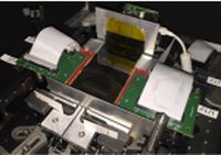
Lockheed Martin’s SPIDER (Segmented Planar Imaging Detector for Electro-optical Reconnaissance) concept trades bulky lenses and telescopes for a thin layer of hundreds or thousands of tiny lenses that feed photonic integrated circuits on silicon chips. These photonic circuits, developed by Professor Ben Yoo and his team at UC Davis’ Department of Electrical and Computer Engineering, combine the light from pairs of lenses to construct a digital image from the interference fringes caused by overlapping waves.
SPIDER eyes: Power in numbers
Interference fringes appear when waves coming from the same source through slightly different routes overlap. Think about ripples spreading in a pond. Where peaks or troughs coincide, they reinforce each other; where a peak meets a trough, they cancel out. When the waves originally came from the same source, the resulting interference patterns can yield information about their original state.
Large-scale astronomical interferometer arrays are already used to form ultra-high-resolution images of objects in space from optical and radio telescopes. The goal of SPIDER is to shrink that concept to a thin layer of thousands of lenses feeding silicon chips that can process photons.
Page 1 of 2


