


 It’s Only Common Sense: The Phone Is Still Mightier Than the Keyboard
 The Marketing Minute: Marketing With Layers


Spin Dynamics in an Atomically Thin Semiconductor
February 2, 2016 | NUSEstimated reading time: 2 minutes
Researchers at the National University of Singapore (NUS) and Yale-NUS College have established the mechanisms for spin motion in molybdenum disulfide, an emerging two-dimensional (2D) material. Their discovery resolves a research question on the properties of electron spin in single layers of 2D materials, and paves the way for the next generation of spintronics and low-power devices. The work was published online in the journal Physical Review Letters on 29 January 2016.
Molybdenum disulfide (MoS2), a class of transition metal dichalcogenide compounds, has attracted great attention due to wide recognition of its potential for manipulating novel quantum degrees of freedom such as spin and valley. Due to its unique material properties, a single layer of MoS2 has the potential to be used for spin transistors, where both electric current and spin current can be switched on and off independently. Despite this potential for application, there have not been any experimental studies on the mechanism for spin dynamics in MoS2.
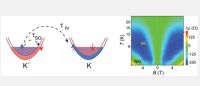
To address this gap, scientists from the Centre for Advanced 2D Materials at NUS used highly precise measurements of the classical and quantum motion of electrons to extract information on how long spins live in this new material.
The team of scientists led by Assistant Professor Goki Eda, co-leader of this study who is from the NUS Department of Physics and Department of Chemistry, thinned down a crystal of molybdenite, a mineral of MoS2, to less than one nanometer. Here, the electrons live in a purely 2D plane that is just one atom thick. The researchers then successfully injected a high density of electrons in this ultra-thin material to enable measurements in the quantum mechanical regime. Quantum transport measurements at low temperatures of 2 Kelvin ( 271 degrees Celsius) revealed a surprising transition, where quantum mechanical wave interference switched from constructive to destructive with increasing magnetic field.
Mr Indra Yudhistira, a Research Associate with the NUS Department of Physics who is under the supervision of Assistant Professor Shaffique Adam, co-leader of the NUS study who is from Yale-NUS College and NUS Department of Physics, demonstrated that this crossover was caused by spin dynamics.
By comparing the theoretical and experimental results, the two research groups were able to extract spin lifetimes and also determine that the relaxation was driven by the Dyakonov-Perel type where electron spins live longer in dirtier samples.
"Aside from investigating the fundamental properties of low field magnetotransport in molybdenum disulfide, our team was able to establish the mechanism for spin scattering to reveal the properties of the electron spin," said Dr Hennrik Schmidt, who was a Research Fellow working under the supervision of Asst Prof Eda when the study was conducted.
Commenting on the significance of the discovery, Asst Prof Adam noted that spin-based devices would generally lead to lower energy consumption as compared to conventional electronics. He explained, "The combination of MoS2 being a semiconductor and the long spin lifetimes open up opportunities in spintronics, where the electron spin and not the electron charge is used to transport information. Such unconventional devices could allow for next generation low-power devices."
Professor Yoshihiro Iwasa, Director of the Center for Quantum-Phase Electronics at the University of Tokyo, and a world expert on quantum devices who first reported superconductivity in this class of materials remarked, "2D materials have been anticipated as a promising platform for spintronics. I feel that this very comprehensive study of the analysis of the electron spin life time will provide crucial information for further pushing the research toward the realisation of a new generation of spintronic devices."
Share on:


Testimonial
"In a year when every marketing dollar mattered, I chose to keep I-Connect007 in our 2025 plan. Their commitment to high-quality, insightful content aligns with Koh Young’s values and helps readers navigate a changing industry. "
Brent Fischthal - Koh YoungSuggested Items
ITW EAE Despatch Ovens Now Support ASTM 5423 Testing
10/15/2025 | ITW EAEAs the demand for high-performance electrical insulation materials continues to grow—driven by the rapid expansion of electric vehicles (EVs) and energy storage systems—thermal processing has become a critical step in material development.
Beyond Thermal Conductivity: Exploring Polymer-based TIM Strategies for High-power-density Electronics
10/13/2025 | Padmanabha Shakthivelu and Nico Bruijnis, MacDermid Alpha Electronics SolutionsAs power density and thermal loads continue to increase, effective thermal management becomes increasingly important. Rapid and efficient heat transfer from power semiconductor chip packages is essential for achieving optimal performance and ensuring long-term reliability of temperature-sensitive components. This is particularly crucial in power systems that support advanced applications such as green energy generation, electric vehicles, aerospace, and defense, along with high-speed computing for data centers and artificial intelligence (AI).
Is Glass Finally Coming of Age?
10/13/2025 | Nolan Johnson, I-Connect007Substrates, by definition, form the base of all electronic devices. Whether discussing silicon wafers for semiconductors, glass-and-epoxy materials in printed circuits, or the base of choice for interposers, all these materials function as substrates. While other substrates have come and gone, silicon and FR-4 have remained the de facto standards for the industry.
Creative Materials to Showcase Innovative Functional Inks for Medical Devices at COMPAMED 2025
10/09/2025 | Creative Materials, Inc.Creative Materials, a leading manufacturer of high-performance functional inks and coatings, is pleased to announce its participation in COMPAMED 2025, taking place November 17–20 in Düsseldorf, Germany.
Jiva Leading the Charge Toward Sustainable Innovation
09/30/2025 | Marcy LaRont, PCB007 MagazineEnvironmental sustainability in business—product circularity—is a high priority these days. “Circularity,” the term meant to replace “recycling,” in its simplest definition, describes a full circle life for electronic products and all their elements. The result is re-use or a near-complete reintroduction of the base materials back into the supply chain, leaving very little left for waste. For what cannot be reused productively, the ultimate hope is to have better, less harmful means of disposal and/or materials that can seamlessly and harmlessly decompose and integrate back into the natural environment. That is where Jiva and Soluboard come in.