


 Dan’s Biz Bookshelf: Four Important Books You Need to Read (Not Just Say You Have)
 The Marketing Minute: Cracking the Code of Technical Marketing


'Lasers Rewired': Scientists Find a New Way to Make Nanowire Lasers
February 12, 2016 | Lawrence Berkeley National LaboratoryEstimated reading time: 4 minutes
Scientists at the U.S. Department of Energy’s Lawrence Berkeley National Laboratory (Berkeley Lab) and UC Berkeley have found a simple new way to produce nanoscale wires that can serve as tiny, tunable lasers.
The nanowires, with diameters as small as 200 nanometers (billionths of a meter) and a blend of materials that has also proven effective in next-generation solar cell designs, were shown to produce very bright, stable laser light. Researchers say the excellent performance of these tiny lasers is promising for the field of optoelectronics, which is focused on combining electronics and light to transmit data, among other applications.
Light can carry far more data, far more rapidly than standard electronics—a single fiber in a fiber-optic cable, measuring less than a hair’s width in diameter, can carry tens of thousands of telephone conversations at once, for example. And miniaturizing lasers to the nanoscale could further revolutionize computing by bringing light-speed data transmission to desktop and ultimately handheld computing devices.
“What’s amazing is the simplicity of the chemistry here,” said Peidong Yang, a chemist in Berkeley Lab’s Materials Sciences Division who led the research, published Feb. 9 in Proceedings of the National Academy of Sciences. More standard techniques that produce nanowires can require expensive equipment and exotic conditions, such as high temperatures, and can suffer from other shortcomings.
The research team developed a simple chemical-dipping solution process to produce a self-assembled blend of nanoscale crystals, plates and wires composed of cesium, lead and bromine (with the chemical formula: CsPbBr3). The same chemical blend, with a molecular architecture composed of cube-like crystal structures, has also proven effective in an emerging wave of new designs for high-efficiency solar cells.
“Most of the earlier work with these types of materials is focused on these solar energy applications,” said Yang, who also holds appointments with UC Berkeley and the Kavli Energy NanoScience Institute at Berkeley Lab and UC Berkeley. “There has been so much progress with these materials in just the past several years—I have a feeling these materials will open a new research frontier for optoelectronics as well,” he said, and in the broader field of photonics, which is focused on using light for a range of applications.
“The whole purpose of developing nano-sized lasers is to interface photonic (light-based) devices with electronic devices seamlessly,” Yang said, “at scales relevant to today’s computer chips. Today, these photonic devices can be bulky.”
Yang’s research team pioneered the development of nanowire lasers almost 15 years ago using a different blend of materials, including zinc oxide (ZnO) and gallium nitride (GaN). But these and other, more conventional combinations of materials used to make nanolasers have shortcomings that can include limited tunability, low brightness or costly manufacturing processes.
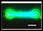
In this latest work, the research team discovered how to produce nanowires by dipping a thin lead-containing film into a methanol solution containing cesium, bromine and chlorine heated to about 122 degrees Fahrenheit. A mix of cesium lead bromide crystalline structures formed, including nanowires with a diameter from 200 to 2,300 nanometers (0.2 to 2.3 microns) and a length ranging from 2 to 40 microns.
A nanowire construction zone: This scanning electron microscope image shows a collection of cesium lead bromide (CsPgbBr3) nanowires and nanoplates grown from a chemical-dipping process. To produce these structures, researchers dipped a thin lead-containing film into a methanol solution containing cesium, bromine and chlorine heated to about 122 degrees. The white scale bar at the lower right represents 10 microns. The image at the bottom left shows the well-formed rectangular end of a nanowire—the white scale bar associated with it represents 500 nanometers. (Credit: Sam Eaton/UC Berkeley)
Select nanowires used in the experiment were placed on a quartz base and excited by another laser source that caused them to emit light. Researchers found that the nanowire lasers emitted light for over 1 billion cycles after being hit by an ultrafast pulse of visible, violet light that lasted just hundredths of quadrillionths of seconds, which Yang said demonstrated remarkable stability.
Yang said to his knowledge these nanowires may be the first to emit laser light using a totally inorganic (not containing carbon) blend of materials. Researchers demonstrated that the nanowire lasers could be tuned to a range of light including visible green and blue wavelengths.
The nanowires have a crystal structure that resembles that of a naturally occurring mineral known as perovskite. Researchers studied their structure with a technique known as transmission electron microscopy at the National Center for Electron Microscopy, part of Berkeley Lab’s Molecular Foundry. The Molecular Foundry is a DOE Office of Science User Facility.
The nanowires’ crystalline structure is a lot like salt, which does make them susceptible to damage from moisture in the air, Yang said.
“That is one weakness—something we have to study and understand how to improve,” he said. It may be possible to coat the nanowires with polymers or other material to make them more damage-resistant, he said. There are also opportunities to test out other materials and learn whether they improve performance, he said, such as substituting tin for lead.
Ted Sargent, a nanotechnology researcher and professor at University of Toronto who is familiar with the study, said, “The results indicate significant promise for perovskite nanomaterials in lasing.” Also, he said, the stability of the nanolasers, which were shown to operate in air for more than an hour, was “impressive.”
Yang said, “This field is rapidly evolving. We just jumped into this field only 12 months ago, and these lasers are already amazing, bright emitters. It’s just so exciting.”
The work was supported by the DOE Office of Science, the Camille and Henry Dreyfus Foundation, and Suzhou Industrial Park. DOE Office of Science support came partly through the Joint Center for Artificial Photosynthesis, a DOE Energy Innovation Hub led by the California Institute of Technology in partnership with Berkeley Lab.
Share on:


Testimonial
"We’re proud to call I-Connect007 a trusted partner. Their innovative approach and industry insight made our podcast collaboration a success by connecting us with the right audience and delivering real results."
Julia McCaffrey - NCAB GroupSuggested Items
Meet the Author Podcast: Martyn Gaudion Unpacks the Secrets of High-Speed PCB Design
07/16/2025 | I-Connect007In this special Meet the Author episode of the On the Line with… podcast, Nolan Johnson sits down with Martyn Gaudion, signal integrity expert, managing director of Polar Instruments, and three-time author in I-Connect007’s popular The Printed Circuit Designer’s Guide to... series.
Intervala Hosts Employee Car and Motorcycle Show, Benefit Nonprofits
08/27/2024 | IntervalaIntervala hosted an employee car and motorcycle show, aptly named the Vala-Cruise and it was a roaring success! Employees had the chance to show off their prized wheels, and it was incredible to see the variety and passion on display.
KIC Honored with IPC Recognition for 25 Years of Membership and Contributions to Electronics Manufacturing Industry
06/24/2024 | KICKIC, a renowned pioneer in thermal process and temperature measurement solutions for electronics manufacturing, is proud to announce that it has been recognized by IPC for 25 years of membership and significant contributions to electronics manufacturing.
Boeing Starliner Spacecraft Completes Successful Crewed Docking with International Space Station
06/07/2024 | BoeingNASA astronauts Barry "Butch" Wilmore and Sunita "Suni" Williams successfully docked Boeing's Starliner spacecraft to the International Space Station (ISS), about 26 hours after launching from Cape Canaveral Space Force Station.
KIC’s Miles Moreau to Present Profiling Basics and Best Practices at SMTA Wisconsin Chapter PCBA Profile Workshop
01/25/2024 | KICKIC, a renowned pioneer in thermal process and temperature measurement solutions for electronics manufacturing, announces that Miles Moreau, General Manager, will be a featured speaker at the SMTA Wisconsin Chapter In-Person PCBA Profile Workshop.