


 Dan’s Biz Bookshelf: Four Important Books You Need to Read (Not Just Say You Have)
 The Marketing Minute: Cracking the Code of Technical Marketing


Silicon Chip with Integrated Laser: Light from a Nanowire
February 12, 2016 | TECHNICAL UNIVERSITY OF MUNICH (TUM)Estimated reading time: 3 minutes
Physicists at the Technical University of Munich (TUM) have developed a nanolaser, a thousand times thinner than a human hair. Thanks to an ingenious process, the nanowire lasers grow right on a silicon chip, making it possible to produce high-performance photonic components cost-effectively. This will pave the way for fast and efficient data processing with light in the future.
Ever smaller, ever faster, ever cheaper -- since the start of the computer age the performance of processors has doubled on average every 18 months. 50 years ago already, Intel co-founder Gordon E. Moore prognosticated this astonishing growth in performance. And Moore's law seems to hold true to this day.
But the miniaturization of electronics is now reaching its physical limits. "Today already, transistors are merely a few nanometers in size. Further reductions are horrendously expensive," says Professor Jonathan Finley, Director of the Walter Schottky Institute at TUM. "Improving performance is achievable only by replacing electrons with photons, i.e. particles of light."
Photonics -- the silver bullet of miniaturization
Data transmission and processing with light has the potential of breaking the barriers of current electronics. In fact, the first silicon-based photonics chips already exist. However, the sources of light for the transmission of data must be attached to the silicon in complicated and elaborate manufacturing processes. Researchers around the world are thus searching for alternative approaches.
Scientists at the TU Munich have now succeeded in this endeavor: Dr. Gregor Koblmüller at the Department of Semiconductor Quantum-Nanosystems has, in collaboration with Jonathan Finley, developed a process to deposit nanolasers directly onto silicon chips. A patent for the technology is pending.
Growing a III-V semiconductor onto silicon requires tenacious experimentation. "The two materials have different lattice parameters and different coefficients of thermal expansion. This leads to strain," explains Koblmüller. "For example, conventional planar growth of gallium arsenide onto a silicon surface results therefore in a large number of defects."
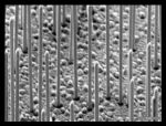
The TUM team solved this problem in an ingenious way: By depositing nanowires that are freestanding on silicon their footprints are merely a few square nanometers. The scientists could thus preclude the emerging of defects in the GaAs material.
Atom by atom to a nanowire
But how do you turn a nanowire into a vertical-cavity laser? To generate coherent light, photons must be reflected at the top and bottom ends of the wire, thereby amplifying the light until it reaches the desired threshold for lasing.
To fulfil these conditions, the researchers had to develop a simple, yet sophisticated solution: "The interface between gallium arsenide and silicon does not reflect light sufficiently. We thus built in an additional mirror -- a 200 nanometer thick silicon oxide layer that we evaporated onto the silicon," explains Benedikt Mayer, doctoral candidate in the team led by Koblmüller and Finley. "Tiny holes can then be etched into the mirror layer. Using epitaxy, the semiconductor nanowires can then be grown atom for atom out of these holes."
Only once the wires protrude beyond the mirror surface they may grow laterally -- until the semiconductor is thick enough to allow photons to jet back and forth to allow stimulated emission and lasing. "This process is very elegant because it allows us to position the nanowire lasers directly also onto waveguides in the silicon chip," says Koblmüller.
Basic research on the path to applications
Currently, the new gallium arsenide nanowire lasers produce infrared light at a predefined wavelength and under pulsed excitation. "In the future we want to modify the emission wavelength and other laser parameters to better control temperature stability and light propagation under continuous excitation within the silicon chips," adds Finley.
The team has just published its first successes in this direction. And they have set their sights firmly on their next goal: "We want to create an electric interface so that we can operate the nanowires under electrical injection instead of relying on external lasers," explains Koblmüller.
"The work is an important prerequisite for the development of high-performance optical components in future computers," sums up Finley. "We were able to demonstrate that manufacturing silicon chips with integrated nanowire lasers is possible."
Share on:


Testimonial
"The I-Connect007 team is outstanding—kind, responsive, and a true marketing partner. Their design team created fresh, eye-catching ads, and their editorial support polished our content to let our brand shine. Thank you all! "
Sweeney Ng - CEE PCBSuggested Items
Summit Interconnect Announces Appointment of Leo LaCroix as Chief Operating Officer
09/09/2025 | Summit Interconnect, Inc.Summit Interconnect, a leading North American manufacturer of Printed Circuit Boards (PCBs), today announced that Leo LaCroix has assumed the role of Chief Operating Officer (COO).
UHDI Fundamentals: UHDI Technology and Industry 4.0
09/03/2025 | Anaya Vardya, American Standard CircuitsUltra high density interconnect (UHDI) technology is rapidly transforming how smart systems are designed and deployed in the context of Industry 4.0. With its capacity to support highly miniaturized, high-performance, and densely packed electronics, UHDI is a critical enabler of the smart, connected, and automated industrial future. Here, I’ll explore the synergy between UHDI and Industry 4.0 technologies, highlighting applications, benefits, and future directions.
Mastering PCB Floor Planning
08/28/2025 | Stephen V. Chavez, Siemens EDAPlacement of PCB components is far more than just fitting components onto a board. It’s a strategic and critical foundational step, often called “floor planning,” that profoundly impacts the board’s performance, reliability, manufacturability, and cost. Floor planning ties into the solvability perspective, with performance and manufacturability being the other two competing perspectives for addressing and achieving success in PCB design.
Macronix Introduces Cutting-Edge Secure-Boot NOR Flash Memory
08/08/2025 | PRNewswireMacronix International Co., Ltd., a leading integrated device manufacturer in the non-volatile memory (NVM) market, announced ArmorBoot MX76, a robust NOR flash memory combining in a single device, the essential performance and an array of security features that deliver rapid boot times and iron-clad data protection.
UHDI Fundamentals: UHDI Technology and Industry 4.0
08/05/2025 | Anaya Vardya, American Standard CircuitsUltra high density interconnect (UHDI) technology is rapidly transforming how smart systems are designed and deployed in Industry 4.0. With its capacity to support highly miniaturized, high-performance, and densely packed electronics, UHDI is a critical enabler of the smart, connected, and automated industrial future. This article explores the synergy between UHDI and Industry 4.0 technologies, highlighting applications, benefits, and future directions.