


 Dan’s Biz Bookshelf: Four Important Books You Need to Read (Not Just Say You Have)
 The Marketing Minute: Cracking the Code of Technical Marketing


Engineering Material Magic
February 15, 2016 | University of UtahEstimated reading time: 2 minutes
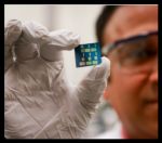
University of Utah engineers have discovered a new kind of 2D semiconducting material for electronics that opens the door for much speedier computers and smartphones that also consume a lot less power.
The semiconductor, made of the elements tin and oxygen, or tin monoxide (SnO), is a layer of 2D material only one atom thick, allowing electrical charges to move through it much faster than conventional 3D materials such as silicon. This material could be used in transistors, the lifeblood of all electronic devices such as computer processors and graphics processors in desktop computers and mobile devices. The material was discovered by a team led by University of Utah materials science and engineering associate professor Ashutosh Tiwari. A paper describing the research was published online Monday, Feb. 15, 2016 in the journal, Advanced Electronic Materials. The paper, which also will be the cover story on the printed version of the journal, was co-authored by University of Utah materials science and engineering doctoral students K. J. Saji and Kun Tian, and Michael Snure of the Wright-Patterson Air Force Research Lab near Dayton, Ohio.
Transistors and other components used in electronic devices are currently made of 3D materials such as silicon and consist of multiple layers on a glass substrate. But the downside to 3D materials is that electrons bounce around inside the layers in all directions.
The benefit of 2D materials, which is an exciting new research field that has opened up only about five years ago, is that the material is made of one layer the thickness of just one or two atoms. Consequently, the electrons "can only move in one layer so it's much faster," says Tiwari.
While researchers in this field have recently discovered new types of 2D material such as graphene, molybdenun disulfide and borophene, they have been materials that only allow the movement of N-type, or negative, electrons. In order to create an electronic device, however, you need semiconductor material that allows the movement of both negative electrons and positive charges known as "holes." The tin monoxide material discovered by Tiwari and his team is the first stable P-type 2D semiconductor material ever in existence.
"Now we have everything -- we have P-type 2D semiconductors and N-type 2D semiconductors," he says. "Now things will move forward much more quickly."
Now that Tiwari and his team have discovered this new 2D material, it can lead to the manufacturing of transistors that are even smaller and faster than those in use today. A computer processor is comprised of billions of transistors, and the more transistors packed into a single chip, the more powerful the processor can become.
Transistors made with Tiwari's semiconducting material could lead to computers and smartphones that are more than 100 times faster than regular devices. And because the electrons move through one layer instead of bouncing around in a 3D material, there will be less friction, meaning the processors will not get as hot as normal computer chips. They also will require much less power to run, a boon for mobile electronics that have to run on battery power. Tiwari says this could be especially important for medical devices such as electronic implants that will run longer on a single battery charge.
"The field is very hot right now, and people are very interested in it," Tiwari says. "So in two or three years we should see at least some prototype device."
Share on:


Testimonial
"We’re proud to call I-Connect007 a trusted partner. Their innovative approach and industry insight made our podcast collaboration a success by connecting us with the right audience and delivering real results."
Julia McCaffrey - NCAB GroupSuggested Items
Curing and Verification in PCB Shadow Areas
09/17/2025 | Doug Katze, DymaxDesign engineers know a simple truth that often complicates electronics manufacturing: Light doesn’t go around corners. In densely populated PCBs, adhesives and coatings often fail to fully cure in shadowed regions created by tall ICs, connectors, relays, and tight housings.
Marcy’s Musings: Advancing the Advanced Materials Discussion
09/17/2025 | Marcy LaRont -- Column: Marcy's MusingsAs the industry’s most trusted global source of original content about the electronics supply chain, we continually ask you about your concerns, what you care about, and what you most want to learn about. Your responses are insightful and valuable. Thank you for caring enough to provide useful feedback and engage in dialogue.
September 2025 PCB007 Magazine: The Future of Advanced Materials
09/16/2025 | I-Connect007 Editorial TeamMoore’s Law is no more, and the advanced material solutions being developed to grapple with this reality are surprising, stunning, and perhaps a bit daunting. Buckle up for a dive into advanced materials and a glimpse into the next chapters of electronics manufacturing.
I-Connect007 Launches Advanced Electronics Packaging Digest
09/15/2025 | I-Connect007I-Connect007 is pleased to announce the launch of Advanced Electronics Packaging Digest (AEPD), a new monthly digital newsletter dedicated to one of the most critical and rapidly evolving areas of electronics manufacturing: advanced packaging at the interconnect level.
Panasonic Industry will Double the Production Capacity of MEGTRON Multi-layer Circuit Board Materials Over the Next Five Years
09/15/2025 | Panasonic Industry Co., Ltd.Panasonic Industry Co., Ltd., a Panasonic Group company, announced plans for a major expansion of its global production capacity for MEGTRON multi-layer circuit board materials today. The company plans to double its production over the next five years to meet growing demand in the AI server and ICT infrastructure markets.