-

- News
- Books
Featured Books
- smt007 Magazine
Latest Issues
Current Issue
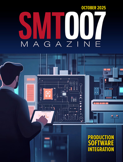
Production Software Integration
EMS companies need advanced software systems to thrive and compete. But these systems require significant effort to integrate and deploy. What is the reality, and how can we make it easier for everyone?

Spotlight on India
We invite you on a virtual tour of India’s thriving ecosystem, guided by the Global Electronics Association’s India office staff, who share their insights into the region’s growth and opportunities.

Supply Chain Strategies
A successful brand is built on strong customer relationships—anchored by a well-orchestrated supply chain at its core. This month, we look at how managing your supply chain directly influences customer perception.
- Articles
- Columns
- Links
- Media kit
||| MENU - smt007 Magazine
ESI Launches Newest Addition to Laser Micromachining Portfolio
February 17, 2016 | ESIEstimated reading time: 2 minutes
Electro Scientific Industries, Inc., an innovator of laser-based manufacturing solutions for the micromachining industry, today introduced the Garnet adaptable laser micromachining platform for high-volume cutting, marking, drilling or engraving applications. Garnet complements ESI’s current micromachining portfolio delivering lower cost of ownership specifically for China manufacturers’ need for larger format materials. The Garnet™ platform’s 300x300mm stage allows manufacturers working with large-format materials to optimize production and service for a wider range of customer needs.
The Garnet™ platform is positioned between the Lumen™ platform, ideal for high-end prototyping and production applications where precision and flexibility are paramount, and the lower-cost Jade™ platform, introduced earlier this year for less demanding general purpose laser machining applications.
The Garnet™ platform drives down total cost of ownership by combining ESI’s engineering expertise with China’s manufacturing cost advantages. To meet the market’s wide range of application needs, Garnet™ is built on a versatile base frame capable of multiple laser engine and optics combinations. The Garnet™ platform can be configured and delivered rapidly to meet the short product ramp times of contract manufacturers in China.
“Manufacturers of larger format components in consumer electronics, automotive and soft goods markets have the same range of application needs and pressures to lower their cost of ownership as those manufacturing smaller components in the consumer electronics market,” said Mantreh Nournia, General Manager, Micro Machining Division, ESI. “To meet these market needs and increase manufacturer’s capabilities on large-format materials, we launched the Garnet™ platform as the third system in our micromachining series and ESI’s second system built on a low-cost China platform. Garnet™ extends our expertise with the Jade™ and Lumen™ platforms to address a broad set of laser material interaction applications at a very attractive cost of ownership.”
The Garnet™ platform includes many capabilities found in high-end prototyping tools including superior configuration flexibility, compound beam motion control and the highest levels of precision in the industry for this class of product. Garnet™ lowers overall cost of ownership with a 25 percent jump in placement accuracy compared to other mid-range laser systems.
About ESI
ESI's integrated solutions allow industrial designers and process engineers to control the power of laser light to transform materials in ways that differentiate their consumer electronics, wearable devices, semiconductor circuits and high-precision components for market advantage. ESI's laser-based manufacturing solutions feature the micro-machining industry's highest precision and speed, and target the lowest total cost of ownership. ESI is headquartered in Portland, Ore., with global operations from the Pacific Northwest to the Pacific Rim.
Testimonial
"Our marketing partnership with I-Connect007 is already delivering. Just a day after our press release went live, we received a direct inquiry about our updated products!"
Rachael Temple - AlltematedSuggested Items
Beyond Thermal Conductivity: Exploring Polymer-based TIM Strategies for High-power-density Electronics
10/13/2025 | Padmanabha Shakthivelu and Nico Bruijnis, MacDermid Alpha Electronics SolutionsAs power density and thermal loads continue to increase, effective thermal management becomes increasingly important. Rapid and efficient heat transfer from power semiconductor chip packages is essential for achieving optimal performance and ensuring long-term reliability of temperature-sensitive components. This is particularly crucial in power systems that support advanced applications such as green energy generation, electric vehicles, aerospace, and defense, along with high-speed computing for data centers and artificial intelligence (AI).
Is Glass Finally Coming of Age?
10/13/2025 | Nolan Johnson, I-Connect007Substrates, by definition, form the base of all electronic devices. Whether discussing silicon wafers for semiconductors, glass-and-epoxy materials in printed circuits, or the base of choice for interposers, all these materials function as substrates. While other substrates have come and gone, silicon and FR-4 have remained the de facto standards for the industry.
Creative Materials to Showcase Innovative Functional Inks for Medical Devices at COMPAMED 2025
10/09/2025 | Creative Materials, Inc.Creative Materials, a leading manufacturer of high-performance functional inks and coatings, is pleased to announce its participation in COMPAMED 2025, taking place November 17–20 in Düsseldorf, Germany.
Jiva Leading the Charge Toward Sustainable Innovation
09/30/2025 | Marcy LaRont, PCB007 MagazineEnvironmental sustainability in business—product circularity—is a high priority these days. “Circularity,” the term meant to replace “recycling,” in its simplest definition, describes a full circle life for electronic products and all their elements. The result is re-use or a near-complete reintroduction of the base materials back into the supply chain, leaving very little left for waste. For what cannot be reused productively, the ultimate hope is to have better, less harmful means of disposal and/or materials that can seamlessly and harmlessly decompose and integrate back into the natural environment. That is where Jiva and Soluboard come in.
Space Forge Inc. and United Semiconductors LLC Partner to Develop the Supply Chain for Space-grown Semiconductor Materials
09/29/2025 | Space Forge Inc.Space Forge Inc., the advanced materials company revolutionizing semiconductor manufacturing in space, has announced the signing of a strategic Memorandum of Understanding (MoU) with United Semiconductors LLC, a leading specialist in bulk crystal growth of III-V semiconductor compounds. The agreement formalizes the ongoing collaborative efforts that started over a year ago, marking a significant step forward in strengthening the partnership between the two companies.


