


 Dan’s Biz Bookshelf: Four Important Books You Need to Read (Not Just Say You Have)
 The Marketing Minute: Cracking the Code of Technical Marketing


Researcher's Chiral Graphene Stacks Break New Ground
February 25, 2016 | Cornell UniversityEstimated reading time: 3 minutes
Hands and feet are two examples of chiral objects – non-superimposable mirror images of each other. One image is distinctly “left-handed,” while the other is “right-handed.” A simple drinking glass and a ball are achiral, meaning the object and its mirror image look exactly the same.
In science, chirality is a fundamental concept in a number of disciplines, including medicine. In the 1950s and early ’60s, pregnant women were prescribed the sedative thalidomide, but the drug produced horrific birth defects in thousands of children around the world. The reason: The thalidomide molecule is chiral, and while the left-hand molecule was indeed a sedative, the right-hand one was found later to produce fetal abnormalities.
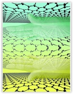
Until very recently, similar “handedness” in large area films with atomic scale precision hadn’t been investigated. The research team of Cornell’s Jiwoong Park has broken new ground in this area, developing a chiral atomically thin film only 2-atoms-thick, through circular stacking of graphene.
This material is of interest in the fields of polarization optics, stereochemistry, optoelectronics and spin transport electronics, or spintronics.
“I would say that we’ve been curious about this for a long time, whether we can make this material,” said Park, associate professor of chemistry and chemical biology and an executive member of the Kavli Institute at Cornell for Nanoscale Science.
The Park group’s paper, “Chiral Atomically Thin Films,” was published Feb. 22 in Nature Nanotechnology. Park and Cheol-Joo Kim, a postdoctoral researcher in chemistry and chemical biology, designed and conducted the experiments and co-wrote the paper.
Contributors include Zack Ziegler ’16, an engineering physics major; former Cornell postdoc Yui Ogawa; and Cecilia Noguez of the Instituto de Fisica, Universidad Nacional Autonoma de Mexico. Noguez is one of the world’s leading computational physicists, and she helped calculate the Park group’s results.
“This discovery and its confirmation may have a lot of implications in both pure and applied science,” Noguez said. “This may be applied for sensing biomolecules, and to induce and control asymmetric catalysis, among others. I am sure this discovery opens new research directions for other 2-D materials.”
For the experiment, Kim and Ogawa grew graphene sheets on copper, then cut them into multiple sheets. Those sheets were then stacked, with each sheet rotated slightly before being placed on the one below it. The rotation went clockwise on one stack and counter-clockwise on the other to form right-handed and left-handed stacks.
Circularly polarized light – alternating left-handed and right-handed beams – were shone onto the stacks, and circular dichroism (or CD, the differential absorption of left- and right-handed light), was measured. It’s the circular dichroism of 3-D glasses that allows you to see a movie in three dimensions.
The special graphene film’s CD was stronger than the group anticipated. After months of hard work and some setbacks, that discovery came around Thanksgiving 2014, and “that was when the whole process accelerated,” Kim said.
But after achieving this atomic-scale breakthrough, the group had to quantify its results, so it turned to Noguez.
“It’s one of those rare cases where we knew exactly what we wanted, so we knew what quantity had to be calculated,” Park said. “It’s not an easy calculation, and we did a lot of research and realized that Cecilia is the best person to do this.”
Noguez admitted her group was initially surprised by Park’s findings, but in analyzing them further realized the research made sense.
“We predicted a long time ago a similar behavior for single-wall carbon nanotubes and more recently in ligand-protected metal nanoparticles,” she said. “So in the end, those results made sense to me.”
The project was supported by the National Science Foundation, through the Cornell Center for Materials Research, and the Air Force Office of Scientific Research. Sample fabrication was performed at the Cornell NanoScale Science and Technology Facility, which is supported by the NSF.
Share on:


Testimonial
"Advertising in PCB007 Magazine has been a great way to showcase our bare board testers to the right audience. The I-Connect007 team makes the process smooth and professional. We’re proud to be featured in such a trusted publication."
Klaus Koziol - atgSuggested Items
Electrodeposited Copper Foils Market to Grow by $11.7 Billion Over 2025-2032
09/18/2025 | Globe NewswireThe global electrodeposited copper foils market is poised for dynamic growth, driven by the rising adoption in advanced electronics and renewable energy storage solutions.
MacDermid Alpha Showcases Advanced Interconnect Solutions at PCIM Asia 2025
09/18/2025 | MacDermid Alpha Electronics SolutionsMacDermid Alpha Electronic Solutions, a global leader in materials for power electronics and semiconductor assembly, will showcase its latest interconnect innovations in electronic interconnect materials at PCIM Asia 2025, held from September 24 to 26 at the Shanghai New International Expo Centre, Booth N5-E30
Trouble in Your Tank: Implementing Direct Metallization in Advanced Substrate Packaging
09/15/2025 | Michael Carano -- Column: Trouble in Your TankDirect metallization systems based on conductive graphite are gaining popularity throughout the world. The environmental and productivity gains achievable with this process are outstanding. Direct metallization reduces the costs of compliance, waste treatment, and legal issues related to chemical exposure. A graphite-based direct plate system has been devised to address these needs.
Closing the Loop on PCB Etching Waste
09/09/2025 | Shawn Stone, IECAs the PCB industry continues its push toward greener, more cost-efficient operations, Sigma Engineering’s Mecer System offers a comprehensive solution to two of the industry’s most persistent pain points: etchant consumption and rinse water waste. Designed as a modular, fully automated platform, the Mecer System regenerates spent copper etchants—both alkaline and acidic—and simultaneously recycles rinse water, transforming a traditionally linear chemical process into a closed-loop system.
Driving Innovation: Depth Routing Processes—Achieving Unparalleled Precision in Complex PCBs
09/08/2025 | Kurt Palmer -- Column: Driving InnovationIn PCB manufacturing, the demand for increasingly complex and miniaturized designs continually pushes the boundaries of traditional fabrication methods, including depth routing. Success in these applications demands not only on robust machinery but also sophisticated control functions. PCB manufacturers rely on advanced machine features and process methodologies to meet their precise depth routing goals. Here, I’ll explore some crucial functions that empower manufacturers to master complex depth routing challenges.