


 Dan’s Biz Bookshelf: Four Important Books You Need to Read (Not Just Say You Have)
 The Marketing Minute: Cracking the Code of Technical Marketing


Artificial Control of Exciplexes Opens Possibilities for New Electronics
February 29, 2016 | Kyushu University, OPERAEstimated reading time: 3 minutes
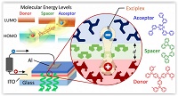
Demonstrating a strategy that could form the basis for a new class of electronic devices with uniquely tunable properties, researchers at Kyushu University were able to widely vary the emission color and efficiency of organic light-emitting diodes based on exciplexes simply by changing the distance between key molecules in the devices by a few nanometers.
This new way to control electrical properties by slightly changing the device thickness instead of the materials could lead to new kinds of organic electronic devices with switching behavior or light emission that reacts to external factors.
Organic electronic devices such as OLEDs and organic solar cells use thin films of organic molecules for the electrically active materials, making flexible and low-cost devices possible.
A key factor determining the properties of organic devices is the behavior of packets of electrical energy called excitons. An exciton consists of a negative electron attracted to a positive hole, which can be thought of as a missing electron.
In OLEDs, the energy in these excitons is released as light when the electron loses energy and fills the vacancy of the hole. Varying the exciton energy, for example, will change the emission color.
However, excitons are commonly localized on a single organic molecule and tightly bound with binding energies of about 0.5 eV. Thus, entirely new molecules must usually be designed and synthesized to obtain different properties from these Frenkel-type excitons, such as red, green, or blue emission for displays.
Researchers at Kyushu University's Center for Organic Photonics and Electronics Research (OPERA) instead focused on a different type of exciton called an exciplex, which is formed by a hole and electron located on two different molecules instead of the same molecule.
By manipulating the molecular distance between the electron-donating molecule (donor) and the electron-accepting molecule (acceptor) that carry the exciplex's hole and electron, respectively, the researchers could modify the properties of these weakly bound excitons.
"What we did is similar to placing sheets of paper between a magnet and a refrigerator," said Associate Professor Hajime Nakanotani, lead author of the paper reporting these results published online February 26, 2016, in the journal Science Advances.
"By increasing the thickness of an extremely thin layer of organic molecules inserted as a spacer between the donor and acceptor, we could reduce the attraction between the hole and electron in the exciplex and thereby greatly influence the exciplex's energy, lifetime, and emission color and efficiency."
Indeed, the changes can be large: by inserting a spacer layer with a thickness of only 5 nm between a donor layer and an acceptor layer in an OLED, the emission color shifted from orange to yellowish green and the light emission efficiency increased 700%.
For this to work, the organic molecule used for the spacer layer must have an excitation energy higher than those of the donor and acceptor, but such materials are already widely available.
While the molecular distance is currently determined by the thickness of the vacuum-deposited spacer layer, the researchers are now looking into other ways to control the distance.
"This gives us a powerful way to greatly vary device properties without redesigning or changing any of the materials," said Professor Chihaya Adachi, director of OPERA. "In the future, we envision new types of exciton-based devices that respond to external forces like pressure to control the distance and electrical behavior."
In addition, the researchers found that the exciplexes were still formed when the spacer was 10 nm thick, which is long on a molecular scale.
"This is some of the first evidence that electrons and holes could still interact like this across such a long distance," commented Professor Adachi, "so this structure may also be a useful tool for studying and understanding the physics of excitons to design better OLEDs and organic solar cells in the future."
"From both scientific and applications standpoints, we are excited to see where this new path for exciton engineering takes us and hope to establish a new category of exciton-based electronics."
Share on:


Testimonial
"The I-Connect007 team is outstanding—kind, responsive, and a true marketing partner. Their design team created fresh, eye-catching ads, and their editorial support polished our content to let our brand shine. Thank you all! "
Sweeney Ng - CEE PCBSuggested Items
Beyond Design: Slaying Signal Integrity Villains
09/17/2025 | Barry Olney -- Column: Beyond DesignHigh-speed PCB design is a balancing act, where subtle oversights can develop into major signal integrity nightmares. Some culprits lie dormant during early validation, only to reveal themselves later through workflow disruptions and elusive performance bottlenecks. Take crosstalk, for example. What begins as a stray signal coupling between traces can ripple through the design, ultimately destabilizing the power distribution network. Each of these troublemakers operates with signature tactics, but they also have well-known vulnerabilities.
Driving Innovation: Depth Routing Processes—Achieving Unparalleled Precision in Complex PCBs
09/08/2025 | Kurt Palmer -- Column: Driving InnovationIn PCB manufacturing, the demand for increasingly complex and miniaturized designs continually pushes the boundaries of traditional fabrication methods, including depth routing. Success in these applications demands not only on robust machinery but also sophisticated control functions. PCB manufacturers rely on advanced machine features and process methodologies to meet their precise depth routing goals. Here, I’ll explore some crucial functions that empower manufacturers to master complex depth routing challenges.
Global PCB Connections: Understanding the General Fabrication Process—A Designer’s Hidden Advantage
08/14/2025 | Markus Voeltz -- Column: Global PCB ConnectionsDesigners don’t need to become fabricators, but understanding the basics of PCB fabrication can save you time, money, and frustration. The more you understand what’s happening on the shop floor, the better you’ll be able to prevent downstream issues. As you move into more advanced designs like HDI, flex circuits, stacked vias, and embedded components, this foundational knowledge becomes even more critical. Remember: the fabricator is your partner.
I-Connect007 Editor’s Choice: Five Must-Reads for the Week
08/08/2025 | Andy Shaughnessy, I-Connect007If you’ve been watching the news lately, you might be tempted to opine, “What’s going on here?” In this week’s must-reads, we have a wrap-up of the latest news about U.S. tariffs with Asia, and columnist Tom Yang explains why some PCB fabrication business should remain in China. We also have a piece that examines the unprecedented growth that green manufacturing is expected to see over the next four years.
Driving Innovation: Inner Layer Alignment Methods in PCB Production
08/06/2025 | Kurt Palmer -- Column: Driving InnovationIn PCB manufacturing, precision is a fundamental requirement. Among many complex processes, the accurate registration of inner layers before lamination is one of the most critical. Much like a child's game where rings must be perfectly stacked onto a single pin, PCB manufacturers align multiple conductive and insulating layers to form a cohesive, functional board. This alignment directly affects PCB precision; tighter layer alignment results in smaller "annular rings," superior performance, and higher yields.