


 Dan’s Biz Bookshelf: Four Important Books You Need to Read (Not Just Say You Have)
 The Marketing Minute: Cracking the Code of Technical Marketing


Researchers Stack the Odds for Novel Optoelectronic 2D Materials
March 3, 2016 | ORNLEstimated reading time: 4 minutes
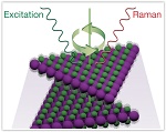
Stacking layers of nanometer-thin semiconducting materials at different angles is a new approach to designing the next generation of energy-efficient transistors and solar cells. The atoms in each layer are arranged in hexagonal arrays. When two layers are stacked and rotated, atoms from one layer overlap with those in the other layer and can form an infinite number of overlapping patterns, like the Moiré patternsthat result when two screens are overlaid and one is rotated on top of the other. Theoretical calculations predict excellent electronic and optical properties for some stacking patterns, but practically, how can these patterns be made and characterized?
Recently a team led by researchers from the Department of Energy’s Oak Ridge National Laboratory used the vibrations between two layers to decipher their stacking patterns. The team employed a method called low-frequency Raman spectroscopy to measure how the layers vibrate with respect to each other and compared the frequencies of the measured vibrations with their theoretically predicted values. Their study provides a platform for engineering two-dimensional (2D) materials with optical and electronic properties that strongly depend on stacking configurations. The findings are published in ACS Nano,a journal of the American Chemical Society.
“Low-frequency Raman spectroscopy, in combination with first-principles modeling, offers a quick and easy approach to reveal complex stacking configurations in the twisted bilayers of a promising semiconductor, without relying on other expensive and time-consuming experimental techniques,” said co-lead author Liangbo Liang, a Wigner Fellow at ORNL. “We are the first to show that low-frequency Raman spectra can be used as fingerprints to characterize the relative layer stacking in semiconducting 2D materials.”
In Raman scattering, an optical method for probing atomic vibrations, a material scatters monochromatic light from a laser. Whereas conventional Raman spectroscopy may probe more than approximately 3 trillion atomic vibrations per second, low-frequency Raman spectroscopy detects vibrations that are an order of magnitude slower. The low-frequency technique is sensitive to weak attractive forces between layers, called van der Waals coupling. It can provide crucial insight about layer thickness and stacking—aspects that govern fundamental properties of 2D materials.
“This work combines state-of-the art synthesis and processing of 2D materials, their unique spectroscopic characterization, and data interpretation using first-principles theory,” said co-lead author Alex Puretzky. “High-resolution Raman spectroscopy that can probe low-frequency modes requires specialized instrumentation, and only a few places around the world have such a capability together with advanced synthesis and characterization tools, and theory and computational modeling expertise. The Center for Nanophase Materials Sciences at ORNL is among them.”
Page 1 of 2
Share on:


Testimonial
"In a year when every marketing dollar mattered, I chose to keep I-Connect007 in our 2025 plan. Their commitment to high-quality, insightful content aligns with Koh Young’s values and helps readers navigate a changing industry. "
Brent Fischthal - Koh YoungSuggested Items
Curing and Verification in PCB Shadow Areas
09/17/2025 | Doug Katze, DymaxDesign engineers know a simple truth that often complicates electronics manufacturing: Light doesn’t go around corners. In densely populated PCBs, adhesives and coatings often fail to fully cure in shadowed regions created by tall ICs, connectors, relays, and tight housings.
Marcy’s Musings: Advancing the Advanced Materials Discussion
09/17/2025 | Marcy LaRont -- Column: Marcy's MusingsAs the industry’s most trusted global source of original content about the electronics supply chain, we continually ask you about your concerns, what you care about, and what you most want to learn about. Your responses are insightful and valuable. Thank you for caring enough to provide useful feedback and engage in dialogue.
September 2025 PCB007 Magazine: The Future of Advanced Materials
09/16/2025 | I-Connect007 Editorial TeamMoore’s Law is no more, and the advanced material solutions being developed to grapple with this reality are surprising, stunning, and perhaps a bit daunting. Buckle up for a dive into advanced materials and a glimpse into the next chapters of electronics manufacturing.
I-Connect007 Launches Advanced Electronics Packaging Digest
09/15/2025 | I-Connect007I-Connect007 is pleased to announce the launch of Advanced Electronics Packaging Digest (AEPD), a new monthly digital newsletter dedicated to one of the most critical and rapidly evolving areas of electronics manufacturing: advanced packaging at the interconnect level.
Panasonic Industry will Double the Production Capacity of MEGTRON Multi-layer Circuit Board Materials Over the Next Five Years
09/15/2025 | Panasonic Industry Co., Ltd.Panasonic Industry Co., Ltd., a Panasonic Group company, announced plans for a major expansion of its global production capacity for MEGTRON multi-layer circuit board materials today. The company plans to double its production over the next five years to meet growing demand in the AI server and ICT infrastructure markets.