


 Dan’s Biz Bookshelf: Four Important Books You Need to Read (Not Just Say You Have)
 The Marketing Minute: Cracking the Code of Technical Marketing


Nanotechnologists at UT Make Orientation of Magnetism Adjustable in New Materials
March 8, 2016 | University of TwenteEstimated reading time: 2 minutes
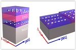
Nanotechnologists at the UT research institute MESA+ are now able to create materials in which they can influence and precisely control the orientation of the magnetism at will. An interlayer just 0.4 nanometres thick is the key to this success. The materials present a range of interesting possibilities, such as a new way of creating computer memory as well as spintronics applications – a new form of electronics that works on the basis of magnetism instead of electricity. The research was published today in the leading scientific journal Nature Materials.
Nanotechnologists at the University of Twente are specialized in creating new materials. Thanks to the top-level facilities at the MESA+ NanoLab they are able to combine materials as they wish, with the ability to control the material composition down to atom level. In particular, they specialize in creating materials composed of extremely thin layers, sometimes just one atom thick.
Computer memory
In research published today in the scientific journal Nature Materials, they show their ability to create new materials within which they can precisely and locally control the orientation of the magnetism. This opens the way to new possibilities of creating computer memory. Moreover, this method of creating materials is interesting for spintronics, a new form of electronics that does not utilize the movement of charges but instead the magnetic properties of a material. This not only makes electronics very fast and efficient, but also allows them to be produced in extremely small dimensions.
Interlayer
In the course of this research the scientists stacked up various thin layers of Perovskite materials. By placing an extremely thin interlayer of just 0.4 nanometres between the layers (a nanometre is a million times smaller than a millimetre), it becomes possible to influence the orientation of the magnetism in the individual Perovskite layers as desired, whereby the orientation of the magnetism in the bottom layer, for instance, is perpendicular to that of the layer above. By varying the location where the interlayer is applied, it becomes possible to select the local orientation of the magnetism anywhere in the material. This is an essential property for new forms of computer memory and for spintronics applications. This effect was already known for much thicker layers, but never before had researchers demonstrated that the orientation of the magnetism can be controlled so precisely with extremely thin layers, too.
Research
The research has been conducted by scientists of the MESA+ research group Inorganic Materials Science in collaboration with colleagues from other institutes, including the University of Antwerp (Belgium), the University of British Columbia (Canada) and TU Wien (Vienna, Austria). Within the research project, the Twente-based researchers were responsible for coordination and for creating the materials. The colleague researchers from Antwerp visualized the materials and were able to image even the smallest atoms in the material. The Canadian researchers created a magnetic cross-section of the material, while the Austrian researchers handled the theoretical calculations.
Share on:


Testimonial
"In a year when every marketing dollar mattered, I chose to keep I-Connect007 in our 2025 plan. Their commitment to high-quality, insightful content aligns with Koh Young’s values and helps readers navigate a changing industry. "
Brent Fischthal - Koh YoungSuggested Items
Curing and Verification in PCB Shadow Areas
09/17/2025 | Doug Katze, DymaxDesign engineers know a simple truth that often complicates electronics manufacturing: Light doesn’t go around corners. In densely populated PCBs, adhesives and coatings often fail to fully cure in shadowed regions created by tall ICs, connectors, relays, and tight housings.
Marcy’s Musings: Advancing the Advanced Materials Discussion
09/17/2025 | Marcy LaRont -- Column: Marcy's MusingsAs the industry’s most trusted global source of original content about the electronics supply chain, we continually ask you about your concerns, what you care about, and what you most want to learn about. Your responses are insightful and valuable. Thank you for caring enough to provide useful feedback and engage in dialogue.
September 2025 PCB007 Magazine: The Future of Advanced Materials
09/16/2025 | I-Connect007 Editorial TeamMoore’s Law is no more, and the advanced material solutions being developed to grapple with this reality are surprising, stunning, and perhaps a bit daunting. Buckle up for a dive into advanced materials and a glimpse into the next chapters of electronics manufacturing.
I-Connect007 Launches Advanced Electronics Packaging Digest
09/15/2025 | I-Connect007I-Connect007 is pleased to announce the launch of Advanced Electronics Packaging Digest (AEPD), a new monthly digital newsletter dedicated to one of the most critical and rapidly evolving areas of electronics manufacturing: advanced packaging at the interconnect level.
Panasonic Industry will Double the Production Capacity of MEGTRON Multi-layer Circuit Board Materials Over the Next Five Years
09/15/2025 | Panasonic Industry Co., Ltd.Panasonic Industry Co., Ltd., a Panasonic Group company, announced plans for a major expansion of its global production capacity for MEGTRON multi-layer circuit board materials today. The company plans to double its production over the next five years to meet growing demand in the AI server and ICT infrastructure markets.