


 Dan’s Biz Bookshelf: Four Important Books You Need to Read (Not Just Say You Have)
 The Marketing Minute: Cracking the Code of Technical Marketing


Researchers Develop Highly Efficient Hollow Copper Electrodes
March 9, 2016 | University of TwenteEstimated reading time: 3 minutes
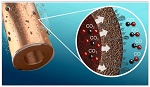
Scientists at the University of Twente research institute MESA+ have developed an electrode in the form of a hollow porous copper fibre which is able to convert carbon dioxide (CO2) into carbon monoxide (CO) extremely efficiently. In principle the invention enables a wide variety of industrial processes, for example in the steel industry, to be made more sustainable. The researchers have applied for a patent on their invention, and their research results have been published in the scientific journal Nature Communications.
Researchers at the University of Twente have developed a hollow copper fibre which can be used to convert CO2 into CO with a very high efficiency. The fibre, which serves as an electrode, is provided with countless minute pores. If the fibre is placed in a bath of water, a voltage potential applied, and CO2 pumped in, the CO2 is converted into CO as it passes out through these pores.
Efficiency and selectivity
The principle is straightforward but the efficiency and selectivity of the reaction are surprisingly high, in part because the electrode provides a huge surface area on which the reaction can take place. An important innovation is the optimized interface between gas, fluid and copper particles, allowing the very efficient supply of CO2 and removal of the product, CO. Conversion takes place at about ten times the rate when using the most advanced copper electrodes currently available, while the selectivity (expressed as the percentage of electrons that actually convert CO2 into CO) is 85%, compared to 35% in current copper electrodes. The newly developed electrode also performs better than electrodes made of expensive precious metals such as gold or silver.
Manufacturing process
The fibres are manufactured in the following way. Small copper particles are added to a polymer solution. This solution is guided through a small, ring-shaped slit in a water bath, in which the polymer solution solidifies into the form of a thin hollow fibre. A thermal treatment is then employed to remove the polymer and partially fuse the copper particles. The result is a copper oxide fibre. Reacting this with hydrogen at a high temperature yields the final product: a hollow, porous copper fibre with a diameter of 1.5mm and a wall thickness of 0.1mm.
Because this manufacturing technique is based on the way polymeric hollow-fibre membranes are currently constructed on a very large scale, e.g. for kidney dialysis equipment, the researchers involved believe it will be relatively easy to produce the new electrode on a commercial scale.
Page 1 of 2
Share on:


Testimonial
"The I-Connect007 team is outstanding—kind, responsive, and a true marketing partner. Their design team created fresh, eye-catching ads, and their editorial support polished our content to let our brand shine. Thank you all! "
Sweeney Ng - CEE PCBSuggested Items
Electrodeposited Copper Foils Market to Grow by $11.7 Billion Over 2025-2032
09/18/2025 | Globe NewswireThe global electrodeposited copper foils market is poised for dynamic growth, driven by the rising adoption in advanced electronics and renewable energy storage solutions.
MacDermid Alpha Showcases Advanced Interconnect Solutions at PCIM Asia 2025
09/18/2025 | MacDermid Alpha Electronics SolutionsMacDermid Alpha Electronic Solutions, a global leader in materials for power electronics and semiconductor assembly, will showcase its latest interconnect innovations in electronic interconnect materials at PCIM Asia 2025, held from September 24 to 26 at the Shanghai New International Expo Centre, Booth N5-E30
Trouble in Your Tank: Implementing Direct Metallization in Advanced Substrate Packaging
09/15/2025 | Michael Carano -- Column: Trouble in Your TankDirect metallization systems based on conductive graphite are gaining popularity throughout the world. The environmental and productivity gains achievable with this process are outstanding. Direct metallization reduces the costs of compliance, waste treatment, and legal issues related to chemical exposure. A graphite-based direct plate system has been devised to address these needs.
Closing the Loop on PCB Etching Waste
09/09/2025 | Shawn Stone, IECAs the PCB industry continues its push toward greener, more cost-efficient operations, Sigma Engineering’s Mecer System offers a comprehensive solution to two of the industry’s most persistent pain points: etchant consumption and rinse water waste. Designed as a modular, fully automated platform, the Mecer System regenerates spent copper etchants—both alkaline and acidic—and simultaneously recycles rinse water, transforming a traditionally linear chemical process into a closed-loop system.
Driving Innovation: Depth Routing Processes—Achieving Unparalleled Precision in Complex PCBs
09/08/2025 | Kurt Palmer -- Column: Driving InnovationIn PCB manufacturing, the demand for increasingly complex and miniaturized designs continually pushes the boundaries of traditional fabrication methods, including depth routing. Success in these applications demands not only on robust machinery but also sophisticated control functions. PCB manufacturers rely on advanced machine features and process methodologies to meet their precise depth routing goals. Here, I’ll explore some crucial functions that empower manufacturers to master complex depth routing challenges.