-

- News
- Books
Featured Books
- design007 Magazine
Latest Issues
Current Issue
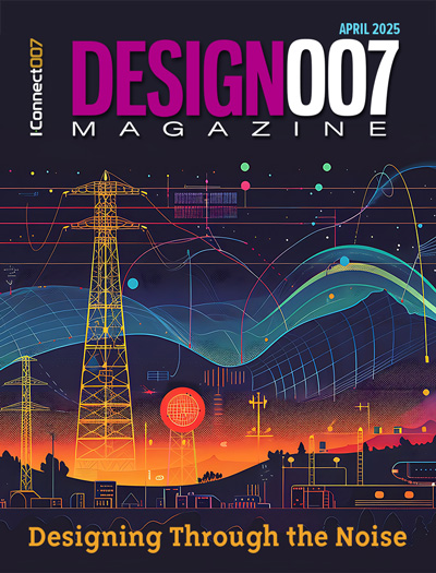
Designing Through the Noise
Our experts discuss the constantly evolving world of RF design, including the many tradeoffs, material considerations, and design tips and techniques that designers and design engineers need to know to succeed in this high-frequency realm.

Learning to Speak ‘Fab’
Our expert contributors clear up many of the miscommunication problems between PCB designers and their fab and assembly stakeholders. As you will see, a little extra planning early in the design cycle can go a long way toward maintaining open lines of communication with the fab and assembly folks.

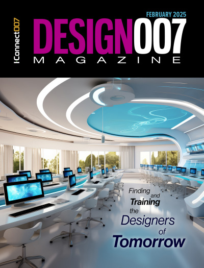
Training New Designers
Where will we find the next generation of PCB designers and design engineers? Once we locate them, how will we train and educate them? What will PCB designers of the future need to master to deal with tomorrow’s technology?
- Articles
- Columns
Search Console
- Links
- Media kit
||| MENU - design007 Magazine
Stadium’s Shanghai Design Centre Pushes Design-led Growth for Wireless Applications
March 11, 2016 | Stadium GroupEstimated reading time: 1 minute
On 16th February 2016, Stadium’s Board of Directors cut the ribbon to signify the official opening ceremony for its Regional Design Centre (RDC) in Shanghai’s Zhangjiang Hi-Tech Park, China.
In support of the Group’s wider strategy to further develop its design-led technology businesses, the Shanghai RDC has become an International Purchasing Office (IPO) and the Company’s regional research and development hub in wireless M2M connectivity for global OEM products in automotive, medical, security and other growing vertical markets. Driven by the Internet of Things (IoT), which continues to stimulate demand, the M2M space is forecast for high growth.
“The new Shanghai Regional Design Centre is an exciting move for Stadium that both strengthens our wireless capabilities and gives us access into new markets,” said Charlie Peppiatt, CEO, Stadium Group. “We have recruited a highly experienced team, including design engineers and field application engineers, specialising in wireless, RF and M2M technologies. Stadium’s presence in China, delivered by the new Shanghai RDC and manufacturing facility in Dongguan, positions the company to capitalise on a growing market opportunity and expand further into the Asia Pacific market.”
A 210 m² site on the Zhangjiang Hi-Tech Park was selected as the location for Stadium’s RDC office. Located on the Pudong side of the city, this high-tech park is host to a large number of industries including integrated circuits, software, IoT development, biopharmaceuticals, information security, semiconductor illumination and modern agriculture, among others. A significant number of multinationals also have their research and development centres located here. The talent pool in Zhangjiang Hi-Tech Park for electronics engineering and related skills is the best in Asia with a vast pool of experienced skilled doctorates and graduates.
Suggested Items
Real Time with... IPC APEX EXPO 2025: Emerging Trends in Design and Technology
04/16/2025 | Real Time with...IPC APEX EXPOAndy Shaughnessy speaks with IPC design instructor Kris Moyer to discuss emerging design trends. They cover UHDI technology, 3D printing, and optical data transmission, emphasizing the importance of a skilled workforce. The role of AI in design is highlighted, along with the need for understanding physics and mechanics as designs become more complex. The conversation concludes with a focus on enhancing math skills for better signal integrity.
Electronic System Design Industry Posts $4.9 Billion in Revenue in Q4 2024
04/15/2025 | SEMIElectronic System Design (ESD) industry revenue increased 11% to $4,927.3 million in the fourth quarter of 2024 from the $4440.9 million reported in the fourth quarter of 2023, the ESD Alliance, a SEMI Technology Community, announced in its latest Electronic Design Market Data (EDMD) report.
Connect the Dots: Involving Manufacturers Earlier Prevents Downstream Issues
04/16/2025 | Matt Stevenson -- Column: Connect the DotsIf you have read any of my earlier columns, you know I am passionate about helping designers design for the reality of manufacturing. Designing for manufacturability (DFM) is a team sport. DFM is a design process that looks forward to the manufacturing process and integrates with it so that manufacturing requirements and capabilities can be accurately reflected in the design work.
Würth Elektronik ICS at PCIM Europe 2025
04/14/2025 | Wurth ElektronikWürth Elektronik ICS will be exhibiting at PCIM in Nuremberg from 6 to 8 May 2025. The specialist for PCB connection solutions in the high-current sector and inventor of Powerelements will be focussing on power electronics at exhibition stand 337 in hall A6.
EDA Tools and RF Design Techniques
04/14/2025 | Andy Shaughnessy, Design007 MagazineHigh-speed PCB design is complex enough, but RF design can be a whole new ball game. RF designers have to contend with tuning and other ideas that traditional PCB designers don’t have to worry about, as well as crosstalk, parasitic capacitance, and material limitations. Most PCB design tool companies now offer RF design options, so designers no longer have to use pureplay RF design tools for anything but the most cutting-edge designs. Cadence Design Systems expanded its RF EDA offerings by acquiring the RF software company AWR a few years ago. We asked David Vye, product management director at Cadence, to share his thoughts on EDA software, RF design, and what new RF designers and engineers need to understand.


