


 The Marketing Minute: If Your Marketing Budget Gets Cut in Half, Then What?
 Punching Out: How Are the Big Boys in Electronics Doing?
 It’s Only Common Sense: Complexity Is the Enemy of Profit


Orbotech Showcases Its Latest Nuvogo 1000 DI System at APEX
March 15, 2016 | OrbotechEstimated reading time: 2 minutes
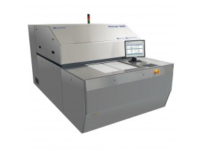
At IPC this week, Orbotech is exhibiting its new Nuvogo 1000 Direct Imaging (DI) system for the PCB manufacturing process. At the show, Orbotech is also presenting, Automated Optical Shaping (AOS) technology.
Orbotech Nuvogo 1000 DI solution brings high accuracy and fast throughput to demanding designs for patterning, solder mask and flex solder mask applications. Utilizing a high-power laser and Orbotech’s unique MultiWave Laser Technology™, the Nuvogo 1000 delivers optimized structures, small undercut and excellent side walls. The high depth-of-focus achieved by field-proven Orbotech Large Scan Optics (LSO) technology ensures unmatched quality on the most challenging surface topographies. The system also offers advanced scaling modes for high precision registration, and a dual table mechanism to optimize imaging time and maximize throughput.
Consistently developing new technologies to improve processes and reduce costs, Orbotech will demonstrate Automated Optical Shaping technology which completes patterns where copper is missing with high precision. This technology, intended to be included in future Orbotech solutions, complements Orbotech’s revolutionary CLS (Closed Loop Shaping) which allows for the accurate removal of excess copper without damaging the laminate.
“The new Nuvogo 1000 DI is another testament to Orbotech’s commitment to bring innovative technologies and cost-effective, high-quality solutions to PCB manufacturers,” said Hadar Himmelman, Orbotech West President. “Furthermore, we believe that our planned AOS technology will soon enable manufacturers to address all defects even in the most advanced PCB designs and to practically eliminate scrap.”
The new Orbotech Nuvogo 1000 system is available now. You can see live demos of the Nuvogo 1000 and learn about Orbotech’s new AOS technology at the IPC APEX EXPO, the premier electronics manufacturing industry event in Las Vegas, NV, Booth #903, March 15-17.
About Orbotech Ltd.
Orbotech Ltd. is a global innovator of enabling technologies used in the manufacture of the world’s most sophisticated consumer and industrial products throughout the electronics and adjacent industries. The Company is a leading provider of yield enhancement and production solutions for electronics reading, writing and connecting, used by manufacturers of printed circuit boards, flat panel displays, advanced packaging, micro-electro-mechanical systems and other electronic components. Virtually every electronic device is produced using Orbotech technology. For more information, click here.
Share on:


Testimonial
"The I-Connect007 team is outstanding—kind, responsive, and a true marketing partner. Their design team created fresh, eye-catching ads, and their editorial support polished our content to let our brand shine. Thank you all! "
Sweeney Ng - CEE PCBSuggested Items
Indium Experts to Address Data Center Thermal Management and Sintering Standards at SMTA Conference
05/13/2026 | Indium CorporationAs a leading materials provider for the advanced electronic packaging market, Indium Corporation® experts will share their technical insight and knowledge on two critical industry topics—data center thermal management and sintering protocols—at the SMTA Electronics in Harsh Environments Conference, May 19-21, in Amsterdam, Netherlands.
KYZEN to Focus on Aqueous and Stencil Cleaning Solutions at SMTA Juarez Expo and Tech Forum
05/12/2026 | KYZENKYZEN, the global leader in innovative environmentally friendly cleaning chemistries, will exhibit at the SMTA Monterrey Expo & Tech Forum scheduled to take place on Thursday, May 21 at Injectronics Convention Center in Ciudad Juarez, Chihuahua.
Knocking Down the Bone Pile: Precision Milling of Underfilled SMT Components
05/13/2026 | Nash Bell -- Column: Knocking Down the Bone PileUnderfill is a polymeric material used to fill the gap between a printed circuit board and the underside of surface-mount area-array packages such as BGA, QFP, and QFN devices, thereby surrounding and protecting the solder interconnections. This material increases the component's reliability when subjected to mechanical impacts and shocks by distributing forces.
BGA Technology Expands Inspection Capabilities with Creative Electron TruView X-ray System
05/08/2026 | BGA TechnologyBGA Technology, a leading provider of advanced electronics testing and inspection services, has enhanced its inspection capabilities with the addition of a Creative Electron TruView™ Simplex X-ray system at its Holbrook, New York facility.
AQUANOX A4727 and A4625 Lead KYZEN Offerings at SMTA Oregon Expo and Tech Forum
05/06/2026 | KYZENKYZEN, the global leader in innovative environmentally responsible cleaning chemistries, will exhibit at the SMTA Oregon Expo and Tech Forum scheduled to take place Thursday, May 19 at the Wingspan Event and Conference Center in Hillsboro, Oregon.