


 Dan’s Biz Bookshelf: ‘Elevate: Push Beyond Your Limits'
 The Marketing Minute: The First Step to More Sales—Marketing
 It’s Only Common Sense: Customer Service Is Sales in Disguise


Ucamco's Photoplotting Goes Nano
March 24, 2016 | UcamcoEstimated reading time: 2 minutes
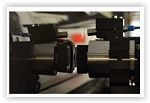
Ucamco is again setting the pace in laser photoplotting with the announcement of its brand-new Nano AF-100 opto-electronics system, which combines with its world-class photoplotting platforms to deliver a spot size of just 1.3 µm, unprecedented resolution capabilities of up to 101,600 ppi, and minimum feature sizes down to a tiny 4µm.
With the optics system's high-speed precision autofocus capabilities, feature accuracy is guaranteed to within 1µm even on large format 1200mm x 1600mm films. The system can be retrofitted to all Barco and Ucamco photoplotters, or provided as an option on all new systems, and is ideal for sectors such as chemical milling, security printing, holograms and flat panel displays, all of which are uncompromising in their demand for ultrafine features and robust, reliable high-speed processes.
Using a powerful array of laser beams and specially designed high-speed Acoustical Optical Modulator and AutoFocus systems, the Nano AF-100 automatically and dynamically controls the intensity, focal point and alignment of each single beam, independently, at speed, and on the fly, delivering the very best in image quality, precision, and productivity.
The Nano AF-100 optics are complemented perfectly by Ucamco's photoplotter platforms, which are recognised throughout the world as being the benchmark for accuracy, throughput and reliability. And they're fast: thanks to Ucamco's multi-core 64-bit FlashRip software, a 460mm x 610mm film can be imaged at maximum resolutions in no more than 15 minutes. Such imaging speeds are made possible by the fact that Ucamco's plotters are built using granite beds as well as contactless movement systems with linear motors and air bearings, guaranteeing rock-solid stability, robustness and repeatability, as well as minimal wear and tear. By the same token, all potential sources of mechanical and thermal film stress have been designed out of the systems' internal film handling systems, ensuring film stability and imaging precision throughout the entire plotting process. These strengths come with a raft of advantages such as ease of use, broad format compatibility, long-term around-the-clock reliability, unparalleled levels of uptime and minimal maintenance needs. It's no wonder that Ucamco photoplotters are the technology of choice for those who are serious about quality, reliability and productivity, and being at the leading edge. They know that Ucamco will keep them there, thanks to its unwavering dedication to engineering excellence, and its ongoing development of technology enablers such as the impressive Nano AF-100 opto-electronics system.
About Ucamco
Ucamco (formerly Barco ETS) is a market leader in PCB CAM software, photoplotting and direct imaging systems, with a global network of sales and support centers. Headquartered in Ghent, Belgium, Ucamco has over 25 years of ongoing experience in developing and supporting leading-edge photoplotters and front-end tooling solutions for the global PCB industry. Key to this success is the company's uncompromising pursuit of engineering excellence in all its products.
Share on:


Suggested Items
Japan’s OHISAMA Project Aims to Beam Solar Power from Space This Year
07/14/2025 | I-Connect007 Editorial TeamJapan could be on the cusp of making history with its OHISAMA project in its quest to become the first country to transmit solar power from space to Earth, The Volt reported.
OSI Systems Receives $34 Million Contract for Cargo and Vehicle Inspection Systems
07/11/2025 | BUSINESS WIREOSI Systems, Inc. announced that its Security division has been awarded a contract worth approximately $34 million by an international customer.
OSI Systems Lands $17 Million Order for Cargo and Vehicle Inspection Systems
07/07/2025 | BUSINESS WIREOSI Systems, Inc. announced that its Security division received an order valued at approximately $17 million from an international customer for cargo and vehicle inspection systems.
KYOCERA AVX Releases New 3DB Hybrid Couplers
07/04/2025 | PRNewswireKYOCERA AVX, a leading global manufacturer of advanced electronic components engineered to accelerate technological innovation and build a better future, released a new line of integrated thin film (ITF) hybrid couplers designed to facilitate the continued evolution of high-frequency wireless systems in industrial, automotive, telecommunications, and telemetry applications.
Driving Innovation: Direct Imaging vs. Conventional Exposure
07/01/2025 | Simon Khesin -- Column: Driving InnovationMy first camera used Kodak film. I even experimented with developing photos in the bathroom, though I usually dropped the film off at a Kodak center and received the prints two weeks later, only to discover that some images were out of focus or poorly framed. Today, every smartphone contains a high-quality camera capable of producing stunning images instantly.