


 Global PCB Connections: Rigid-flex and Flexible PCBs—The Backbone of Modern Electronics
 Flexible Thinking: The Key to a Successful Flex Circuit Design Transfer
 Happy’s Tech Talk #29: Bend-to-Install Semi-flex FR-4


LPKF Launches New Laser Drilling System for Flex Printed Circuits
April 14, 2016 | Pete Starkey, I-Connect007Estimated reading time: 6 minutes
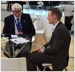
At Laser World of Photonics Exhibition in Shanghai recently, I had a chance to speak with Florian Roick, strategic product manager with LPKF. The company is celebrating a big anniversary this year with the launch of a laser drilling machine to support the specific requirements of the flexible circuit industry. Their equipment can work in single panel or roll-to-roll modes and anticipates future design rules with the capability to drill through and blind vias at diameters of 30 microns and smaller.
Pete Starkey: Florian, I know that the name of LPKF has been associated with the printed circuit industry for more than thirty years, and I believe you're celebrating a big anniversary this year.
Roick: Thanks for having me here. Yes, that's true. This year marks the 40th anniversary of LPKF. We started by inventing a tool that made it possible to replace the etching of the copper for prototyping PCBs, a milling and drilling (mechanical routing) system. Through the years, we progressed to implement lasers to replace the etching process for stencils. In 1992, the first laser stencil cutting machine was presented to the public. Then the laser became an increasingly economical and efficient tool and we started to look into further applications where we could use the laser as a new digital tool, a tool that had no direct contact with the material. We presented several opportunities, such as increased accuracy, for example. We started looking into PCB de-paneling with the laser, and then with the UV laser eventually. Then the scribing of thin film solar cells became a major opportunity and a major market for us as well. Despite being a very difficult market recently, we are the leader in supplying scribing machines all over the world. We saw also a huge success with building three-dimensional circuitry on plastic compound material.
Starkey: This is an area where I am more familiar with your recent developments and applications. I've attended some excellent presentations on the laser structuring of two-dimensional and three-dimensional workpieces.
Roick: The three-dimensional aspect of this new technology allows you to utilize space, for example, in mobile phones, which wasn't occupied by anything functional. All the mobile phone manufacturers now have the chance to use more space inside their systems, and thus reduce size. Reducing size, or the trend of miniaturization, is actually one of the leading requirements in the electronics industry and it's been the reason for us to further develop our technologies. This is also one reason why we looked into the flexible printed circuit (FPC) drilling market.
Starkey: This is something new for you?
Roick: Kind of, yes. As mentioned earlier, we are already involved in the PCB industry with de-paneling, skiving and pocket creation, for example. But we never really had an actual drilling tool available. We were really assessing the situation, the FPC market, and we found that there's a good chance for us to offer a new solution to this industry.
Starkey: So, at this exhibition, you are launching a new drilling system?
Roick: Yes, exactly. This is the MicroLine 5000 drilling system for FPC mainly, and we have launched it here at the Laser World of Photonics and, at the same time, at the IPC APEX EXPO in Las Vegas.
Starkey: My colleagues are attending that show—we have two exhibitions running in parallel this week.
Roick: Yes, so really it's the worldwide product launch of the MicroLine 5000. Of course, the Asian market is where the big production takes place, so it's really a must to have it presented on a worldwide scale.
Starkey: Can you explain the particular characteristics of this machine? What are its unique points?
Roick: As I said, when we were thinking about the FPC drilling market, we asked our customers what their respective needs and requirements were. After evaluating the replies, we realized that yes, we can use all our competencies from LPKF, put them into a new system, and offer customers a system with a very high drilling performance, with the knowledge also that the minimum drilling diameter for future applications could already be achieved. So the unique selling point is very high performance by drilling very small through-holes and blind vias.
Starkey: Can you give us some dimensions?
Roick: Yes. The minimum diameter of a blind via or through-hole measures 30 microns. We utilize a 20-micron laser beam, so it would be possible to go less than 30 microns eventually, depending on the material. We know from our customers’ technical roadmaps that FPC material is becoming thinner and thinner, so holes in the range of 20 microns in diameter are already possible now.
Page 1 of 2
Share on:


Testimonial
"Our marketing partnership with I-Connect007 is already delivering. Just a day after our press release went live, we received a direct inquiry about our updated products!"
Rachael Temple - AlltematedSuggested Items
How Good Design Enables Sustainable PCBs
08/21/2025 | Gerry Partida, Summit InterconnectSustainability has become a key focus for PCB companies seeking to reduce waste, conserve energy, and optimize resources. While many discussions on sustainability center around materials or energy-efficient processes, PCB design is an often overlooked factor that lies at the heart of manufacturing. Good design practices, especially those based on established IPC standards, play a central role in enabling sustainable PCB production. By ensuring designs are manufacturable and reliable, engineers can significantly reduce the environmental impact of their products.
50% Copper Tariffs, 100% Chip Uncertainty, and a Truce
08/19/2025 | Andy Shaughnessy, I-Connect007If you’re like me, tariffs were not on your radar screen until a few months ago, but now political rhetoric has turned to presidential action. Tariffs are front-page news with major developments coming directly from the Oval Office. These are not typical times. President Donald Trump campaigned on tariff reform, and he’s now busy revamping America’s tariff policy.
Global PCB Connections: Understanding the General Fabrication Process—A Designer’s Hidden Advantage
08/14/2025 | Markus Voeltz -- Column: Global PCB ConnectionsDesigners don’t need to become fabricators, but understanding the basics of PCB fabrication can save you time, money, and frustration. The more you understand what’s happening on the shop floor, the better you’ll be able to prevent downstream issues. As you move into more advanced designs like HDI, flex circuits, stacked vias, and embedded components, this foundational knowledge becomes even more critical. Remember: the fabricator is your partner.
MKS’ Atotech to Participate in IPCA Electronics Expo 2025
08/11/2025 | AtotechMKS Inc., a global provider of enabling technologies that transform our world, announced that its strategic brands ESI® (laser systems) and Atotech® (process chemicals, equipment, software, and services) will showcase their latest range of leading manufacturing solutions for printed circuit board (PCB) and package substrate manufacturing at the upcoming 17th IPCA Show to be held at Pragati Maidan, New Delhi from August 21-23, 2025.
MKS Showcases Next-generation PCB Manufacturing Solutions at the Thailand Electronics Circuit Asia 2025
08/06/2025 | MKS Instruments, Inc.MKS Inc, a global provider of enabling technologies that transform our world, today announced its participation in Thailand Electronics Circuit Asia 2025 (THECA 2025), taking place August 20–22 at BITEC in Bangkok.