


 It’s Only Common Sense: Be the Vendor They Compare Everyone Else To
 Marcy’s Musings: Additive Processes, Signal Consequences
 The Marketing Minute: If Your Marketing Budget Gets Cut in Half, Then What?


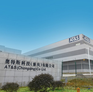
- After Shanghai, another production site opened in China: in the world‘s largest city, Chongqing
- Largest single investment of the AT&S Group, totalling € 480 million; currently 1,700 employees
- Key element in the expansion of technology leadership and further profitable growth of AT&S
- Official opening ceremony with more than 100 guests from politics and business
The site consists of two plants: plant 1 started serial production with one production line in February; plant 2 is currently still being set up. With a total investment volume of roughly € 480 million by 2017, this will be the largest single investment of AT&S to date.
The opening ceremony took place in the presence of representatives of official China and Austria, business, the media, the city of Chongqing, customers, the Supervisory Board and the management of AT&S. The Austrian ambassador in Beijing, Irene Giner-Reichl, Chongqing’s mayor, Huang Qifan, as well as AT&S Supervisory Board Chairman, Hannes Androsch, and CEO Andreas Gerstenmayer held speeches. After the ceremony, selected guests had the opportunity to visit parts of clean room production.
“Chongqing is a key element in the future of AT&S with a view to both technology and positioning, and to further profitable growth. With this plant, we are the first high-end IC substrate manufacturer in China and thus focus on the microelectronics emphasis pursued by the Chinese government at an early stage. Based on the new technologies, combined with the existing high-end technologies, the result is ‘more than AT&S’: we can offer the market new high-end connectivity and advanced packaging solutions and comprehensively position ourselves in the rapidly changing environment of the electronics industry with innovative technologies like IC substrates and wafer level packages for functional modules and the Internet of things. From the PCB top league to the connectivity solution and packaging Champions League, as it were“, says Andreas Gerstenmayer, CEO of AT&S, and adds: “In the medium term, this will entail a new company dimension with revenue of roughly one billion, which will help us to finance future investments from our own cash flow to a greater extent. However, we expect a negative impact during the start-up phase.”
At plant 1, AT&S produces IC substrates, the connection between microchips and printed circuit boards, which are used for microprocessors in computing. Since the start of serial production in late February, the gradual expansion of capacity and the increase in production volume of the complex technology have been proceeding well. From the end of the calendar year 2016, AT&S will gradually start up the second production line for IC substrates. Overall, AT&S will invest roughly € 280 million in property, plant and equipment for this technology by mid-2017.
In addition, the Chongqing site will be extended by a second plant for the latest generation of high-end printed circuit boards, i.e., substrate-like PCBs in order to be able to offer advanced packaging solutions at wafer level. This plant will start production with the first production line in the second half of the calendar year 2016, and with a second production line next year.
Roughly € 200 million will be invested in property, plant and equipment at this plant.
Chen Jian Phua, CEO of the Business Unit Mobile Devices & Substrates, who has been responsible for the establishment of the sites in Shanghai and Chonqing for 12 years for AT&S in leading management positions, outlines the complexity of the technology and the framework conditions: “The new IC substrate technology is not comparable to any technology previously used by AT&S: new, extremely complex production processes in 100 percent cleanroom conditions, new materials as well as a new team, which had to build up know-how in a very short time. We are very proud that we have managed to achieve all this on a very tight schedule. We also invested more than 670,000 hours in training the roughly 1,700 employees who currently work in Chongqing. Sustainable and comprehensive investments in environmental protection have always been important to us at all locations; in Chongqing, about € 24 million have been invested in this area.“
Page 1 of 2


