


 It’s Only Common Sense: The Phone Is Still Mightier Than the Keyboard
 The Marketing Minute: Marketing With Layers


NREL Theory Establishes a Path to High-Performance 2D Semiconductor Devices
April 27, 2016 | NRELEstimated reading time: 2 minutes
Researchers at the Energy Department's National Renewable Energy Laboratory (NREL) have uncovered a way to overcome a principal obstacle in using two-dimensional (2D) semiconductors in electronic and optoelectronic devices.
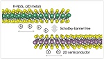
2D semiconductors such as molybdenum disulfide are only a few layers thick and are considered promising candidates for next-generation devices. Scientists first must overcome limitations imposed by a large and tunable Schottky barrier between the semiconductor and a metal contact. The barrier, at the metal/semiconductor junction, creates an obstacle for the flow of electrons or holes through the semiconductor.
The NREL team discovered that the height of the Schottky barrier can be adjusted-or even made to vanish-by using certain 2D metals as electrodes. Such adjustments are not possible with conventional three-dimensional metals because of a strong Fermi level pinning (FLP) effect occurring at the junction of metal and semiconductor, due to electronic states in the semiconductor band gap that are induced by the metal. Increasing the flow of electrons or holes through a semiconductor reduces power losses and improves the device performance.
The NREL theorists considered a family of 2D metals that could bind with the 2D semiconductors through van der Waals interaction. Because this interaction is relatively weak, the metal-induced gap states are suppressed and the FLP effect is negligible. This means that the Schottky barrier becomes highly tunable. By selecting an appropriate 2D metal/2D semiconductor pair, one can reduce the barrier to almost zero (such as H-NbS2/WSe2 for hole conduction).
They noted that using a 2D metal as an electrode would also prove useful for integrating into transparent and flexible electronics because the 2D metal is also transparent and flexible. They also noted that the junction of 2D metal and 2D semiconductor is atomically flat and can have fewer defects, which would reduce carrier scattering and recombination.
The work by Yuanyue Liu, Paul Stradins, and Su-Huai Wei, "Van der Waals metal-semiconductor junction: weak Fermi level pinning enables effective tuning of Schottky barrier," appears in the new issue of Science Advances.
The trio of researchers predicts that hexagonal phase of niobium disulfide (NbS2) is the most promising for hole injection into a 2D semiconductor, and heavily nitrogen-doped graphene can enable efficient electron injection.
This research was funded by the Department of Energy's Office of Energy Efficiency and Renewable Energy. The work used computational resources at NREL and the National Energy Research Scientific Computing Center.
NREL is the U.S. Department of Energy's primary national laboratory for renewable energy and energy efficiency research and development. NREL is operated for the Energy Department by The Alliance for Sustainable Energy, LLC.
Share on:


Testimonial
"In a year when every marketing dollar mattered, I chose to keep I-Connect007 in our 2025 plan. Their commitment to high-quality, insightful content aligns with Koh Young’s values and helps readers navigate a changing industry. "
Brent Fischthal - Koh YoungSuggested Items
Myrias Optics, Pixelligent Announce Strategic Manufacturing Partnership
10/16/2025 | PRNewswireMyrias Optics, a pioneering manufacturer of flat optics , and Pixelligent Technologies LLC, the leading manufacturer of high refractive index (RI) nanocomposites for next-gen electronics, announced that they have entered into a strategic manufacturing partnership.
MacDermid Alpha & Graphic PLC Lead UK’s First Horizontal Electroless Copper Installation
09/30/2025 | MacDermid Alpha & Graphic PLCMacDermid Alpha Electronics Solutions, a leading supplier of integrated materials and chemistries to the electronics industry, is proud to support Graphic PLC, a Somacis company, with the installation of the first horizontal electroless copper metallization process in the UK.
Safran, Rheinmetall Sign Framework Agreement for Advanced Defense Solutions
09/29/2025 | SafranSafran Electronics & Defense and Rheinmetall Electronics have signed a new framework agreement at DSEI London, strengthening their long-term collaboration in the defense sector.
Trouble in Your Tank: Implementing Direct Metallization in Advanced Substrate Packaging
09/15/2025 | Michael Carano -- Column: Trouble in Your TankDirect metallization systems based on conductive graphite are gaining popularity throughout the world. The environmental and productivity gains achievable with this process are outstanding. Direct metallization reduces the costs of compliance, waste treatment, and legal issues related to chemical exposure. A graphite-based direct plate system has been devised to address these needs.
Curtiss-Wright Selected by Rheinmetall to Provide Turret Drive Stabilization System for the KF51 Panther Main Battle Tank
08/11/2025 | BUSINESS WIRECurtiss-Wright announced it has been selected by Rheinmetall Landsysteme Germany (RLS) to provide its modular turret drive stabilization system (TDSS) technology in support of the KF51 Panther Main Battle Tank (MBT).