


 Dan’s Biz Bookshelf: Four Important Books You Need to Read (Not Just Say You Have)
 The Marketing Minute: Cracking the Code of Technical Marketing


Cool Method for Making Waveguides
April 28, 2016 | A*STAREstimated reading time: 2 minutes
Silicon-based films that are useful for waveguides have been made at temperatures low enough to be compatible with standard manufacturing processes. A low-temperature method to produce films based on silicon and nitrogen, which can be used to channel light in devices, has been developed by A*STAR researchers.
Silicon is very a familiar material because of its prevalence in electronic devices, and is increasingly being used in optical and electro-optical devices as well. In particular, it is used to guide light along narrow stripes in components known as waveguides. While silicon has many advantages, it suffers from high losses when used in waveguides as a result of nonlinear absorption at the wavelength used for telecommunications (1,550 nanometers).
One way to reduce these losses is to incorporate nitrogen atoms to produce so-called silicon-rich nitride ― a material whose nitrogen content is intermediate between pure silicon and silicon nitride. But, the usual techniques for making silicon-rich nitride require high temperatures, which renders the process incompatible with the standard technology used for constructing integrated circuits.
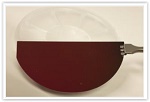
Now, Doris Ng at the A*STAR Data Storage Institute and co-workers have discovered a way to make silicon-rich nitride films (see image) at temperatures as low as 250 degrees Celsius, which is much lower than the temperatures usually used to produce the material. They used a plasma ― a gas that has been energized to the point that electrons have been stripped from its molecules ― to deposit a tailored mixture of silicon and nitrogen atoms onto a substrate.
By changing the process parameters, the researchers were able to vary the refractive index of the films. Under certain conditions, they were able to achieve a high refractive index of 3.08 at the telecommunication wavelength. This refractive index is high enough to make it suitable for use in waveguides, but not high enough to cause detrimental nonlinear effects.
The team demonstrated the potential of their films by making waveguides from them. “The waveguide we made using the silicon-rich nitride with the highest refractive index exhibits very good nonlinear performance,” says Doris.
The study heralds the beginning of a fruitful partnership. “This work is a collaborative project between A*STAR Data Storage Institute and Singapore University of Technology and Design,” notes Ng. “I work on material development, while my collaborator, Dawn Tan, specializes in nonlinear optics. I think it’s the perfect team for our project. We are still at the beginning but have been very encouraged by the results obtained so far.”
The team plans to further optimize the material to reduce losses and hence enhance device performance.
Share on:


Testimonial
"Our marketing partnership with I-Connect007 is already delivering. Just a day after our press release went live, we received a direct inquiry about our updated products!"
Rachael Temple - AlltematedSuggested Items
Electra’s ElectraJet EMJ110 Inkjet Soldermask Now in Black & Blue at Sunrise Electronics
09/08/2025 | Electra Polymers LtdFollowing the successful deployment of Electra’s Green EMJ110 Inkjet Soldermask on KLA’s Orbotech Neos™ platform at Sunrise Electronics in Elk Grove Village, Illinois, production has now moved beyond green.
Magnachip Semiconductor Announces YJ Kim to Step Down as CEO; Current Board Chairman Camillo Martino Appointed Interim CEO
08/14/2025 | PR NewswireMagnachip Semiconductor Corporation today announced that YJ Kim has agreed to step down as CEO and as a member of the Board of Directors, effective immediately. Camillo Martino, Chairman of the Board of Directors, has also been appointed Interim Chief Executive Officer, effective immediately.
Bell to Build X-Plane for Phase 2 of DARPA Speed and Runway Independent Technologies (SPRINT) X-Plane Program
07/09/2025 | Bell Textron Inc.Bell Textron Inc., a Textron Inc. company, has been down-selected for Phase 2 of Defense Advanced Research Projects Agency (DARPA) Speed and Runway Independent Technologies (SPRINT) X-Plane program with the objective to complete design, construction, ground testing and certification of an X-plane demonstrator.
Nolan’s Notes: Moving Forward With Confidence
06/03/2025 | Nolan Johnson -- Column: Nolan's NotesWe’re currently enjoying a revitalized and dynamic EMS provider market with significant growth potential. Since December 2024, the book-to-bill has been extremely strong and growing. Starting with a ratio of 1.24 in December, book-to-bill has continued to accelerate to a 1.41 in April. Yet, there is a global economic restructuring taking place. To say that the back-and-forth with tariffs and trade deals makes for an uncertain market is an understatement. While we may be in a 90-day tariff pause among leading economic nations, the deadline is quickly approaching and that leaves many of you feeling unsettled about what to expect.
Mycronic High Flex Changes Division Name to PCB Assembly Solutions
05/20/2025 | MycronicMycronic AB, the leading Sweden-based electronics assembly solutions provider, announced that its division formerly known as High Flex will now operate under the name PCB Assembly Solutions.