


 Dan’s Biz Bookshelf: ‘Elevate: Push Beyond Your Limits'
 The Marketing Minute: The First Step to More Sales—Marketing
 It’s Only Common Sense: Customer Service Is Sales in Disguise


LDS MIDs: Ready for the Next Generation in Wireless Technology
May 30, 2016 | LPKFEstimated reading time: 2 minutes
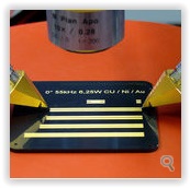
As frequency increases, so do the demands on antenna components. In cooperation with the Institute of High Frequency Technology and Radio Systems (Institut für Hochfrequenztechnik und Funksysteme, HFT) at Leibniz University of Hannover, the LPKF LDS technique is currently being scrutinized for its suitability for next-generation wireless applications.
Publications due for release in late mid-2016 demonstrate the applicability of the LDS technology for antennas in the millimeter-wave frequency band - for example, for fifth-generation (5G) wireless technology or for automotive sensors.
Challenging demands accompanied by increasing device densities and extension of frequency bands mean that flexible approaches are needed to functionalize existing installation space for high-frequency applications. MID technology represents a solution. It allows electrical structures, such as antennas, to be applied to nearly any surface.
Dipl.-Ing. Aline Friedrich, a PhD student at HFT, has worked with 3D-MID technologies for many years: “Three-dimensional antennas offer huge advantages for certain applications. It has already been shown with prototypes that, with the proper layout, three-dimensional antennas represent a powerful alternative to conventional configurations.” The three-dimensional design allows for flexible antenna development so that solutions can be found to meet even the most challenging demands of the future.
HFT uses Laser Direct Structuring (LDS) technology in its development work. With LDS, a laser beam structures a three-dimensional part made of an LDS-doped plastic. The laser beam transfers the desired circuit layout onto the substrate while activating the additive at the same time. In a subsequent electroless metallization step, copper layers are built up on the structures traversed by the laser beam. These layers can then be given various surface finishes.
LDS technology is already established as a preferred manufacturing tech-nique for three-dimensional antennas in the consumer goods sector. LDS antennas covering the frequency band up to 6 GHz, e.g., for Bluetooth, LTE, or Wi-Fi, can be found in many of today’s smartphones, tablets, and wearable devices.
The higher the transmission frequency, the shorter the wavelength - and the greater the demands on the components. The question as to the relevant manufacturing criteria for RF applications beyond 6 GHz formed the basis for the cooperation between HFT and LPKF.
Because next-generation wireless systems for consumer electronics and smart homes are also expected to see an extension of the operating frequency bands to include higher frequencies, one focus of the cooperation is on evaluation and optimization of LDS production for applications in the millimeter-wave frequency band, e.g., for 5G communications technologies. The first prototypes of an antenna for use in millimeter-wave sensors operating at 24 GHz were produced at HFT and measurements verified its success. Production of test antennas operating at 77 GHz is currently underway. The results of the test measurements are also extremely promising for these applications and demonstrate the potential for LDS-based antennas operating at higher frequencies.
Technical papers are expected to be published in late summer 2016. Re-sults will then be discussed through scientific journals and international conferences. Further information can be obtained from Malte Fengler, Product Manager at LPKF.
Share on:


Suggested Items
Elephantech Launches World’s Smallest-Class Copper Nanofiller
07/17/2025 | ElephantechJapanese deep-tech startup Elephantech has launched its cutting-edge 15 nm class copper nanofiller – the smallest class available globally. This breakthrough makes Elephantech one of the first companies in the world to provide such advanced material for commercial use.
Copper Price Surge Raises Alarms for Electronics
07/15/2025 | Global Electronics Association Advocacy and Government Relations TeamThe copper market is experiencing major turbulence in the wake of U.S. President Donald Trump’s announcement of a 50% tariff on imported copper effective Aug. 1. Recent news reports, including from the New York Times, sent U.S. copper futures soaring to record highs, climbing nearly 13% in a single day as manufacturers braced for supply shocks and surging costs.
I-Connect007 Editor’s Choice: Five Must-Reads for the Week
07/11/2025 | Andy Shaughnessy, Design007 MagazineThis week, we have quite a variety of news items and articles for you. News continues to stream out of Washington, D.C., with tariffs rearing their controversial head again. Because these tariffs are targeted at overseas copper manufacturers, this news has a direct effect on our industry.I-Connect007 Editor’s Choice: Five Must-Reads for the Week
Digital Twin Concept in Copper Electroplating Process Performance
07/11/2025 | Aga Franczak, Robrecht Belis, Elsyca N.V.PCB manufacturing involves transforming a design into a physical board while meeting specific requirements. Understanding these design specifications is crucial, as they directly impact the PCB's fabrication process, performance, and yield rate. One key design specification is copper thieving—the addition of “dummy” pads across the surface that are plated along with the features designed on the outer layers. The purpose of the process is to provide a uniform distribution of copper across the outer layers to make the plating current density and plating in the holes more uniform.
Trump Copper Tariffs Spark Concern
07/10/2025 | I-Connect007 Editorial TeamPresident Donald Trump stated on July 8 that he plans to impose a 50% tariff on copper imports, sparking concern in a global industry whose output is critical to electric vehicles, military hardware, semiconductors, and a wide range of consumer goods. According to Yahoo Finance, copper futures climbed over 2% following tariff confirmation.
Copyright © I-Connect007 | IPC Publishing Group Inc. All rights reserved.
Log in