


 Defense Speak Interpreted: Understanding What the Department of Defense Is, and Isn’t
 American Made Advocacy: Rebuilding America’s Military Stockpiles Begins With Microelectronics
 The Right Approach: The End of an Era—DoD Proposes MIL-PRF-31032 Cancellation


A New Way to Control Oxygen for Electronic Properties
June 13, 2016 | Argonne National LaboratoryEstimated reading time: 2 minutes
Hotel managers and materials scientists have a lot in common — they both need to find a way to control properties by managing vacancies.
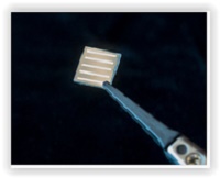
Researchers at the U.S. Department of Energy's (DOE's) Argonne National Laboratory found they could use a small electric current to introduce oxygen voids, or vacancies, that dramatically change the conductivity of thin oxide films. The results are published in Nature Communications.
The discovery improves our understanding of how these materials work and could be useful for new electronics, catalysts or more.
Scientists are always looking for unusual behaviors in materials that could form the basis of new technologies. Oxides are a class of materials that has garnered much recent interest because they sometimes display such unusual behaviors — flipping between insulating and conducting states, turning magnetism on and off or even becoming superconducting: conducting electricity perfectly, without any loss as heat.
We think some of these properties have to do with oxygen vacancies. The structure of an oxide is a repeating crystalline lattice with oxygen atoms peppered throughout, but sometimes there may be voids where an oxygen atom is missing.
The usual way to create oxygen vacancies is by heating the materials and adding or removing oxygen from the environment.
"But the need to control the gas environment limits where and when you can change the material's properties," said Jeff Eastman, an Argonne materials scientist and corresponding author on the paper.
The Argonne team wanted to find out if they could control vacancies with an alternate method.
They built a two-layer material: an indium oxide crystal layer on top of a block of yttria-stabilized zirconia. When the researchers applied a small electric field, they watched the electrical conductivity skyrocket by two orders of magnitude along the boundary where the two layers meet. The effect is reversible; without the field, it reverts back to the initial, less conductive state.
"You could imagine applications for electronics or building catalysts — for example, providing a way to split water or carbon dioxide," Eastman said.
The theory, assisted by computational modeling, is that the difference between the properties of the two materials creates a vertical voltage between them, and negatively charged oxygen ions in the indium oxide are attracted to the flow and move across the interface — leaving vacancies behind.
The team is planning further investigation into whether the same effects occur in other materials and whether the method could control other properties, Eastman said.
The co-authors on the paper, "Interfacial Control of Oxygen Vacancy Doping and Electrical Conduction in Thin Film Oxide Heterostructures," are Argonne scientists Boyd Veal, Peter Zapol, Hakim Iddir, and Peter Baldo, and Seong Keun Kim, an Argonne postdoctoral researcher during this study, now a research scientist at the Korea Institute of Science and Technology.
The team used beamline 12-ID at the Advanced Photon Source, a DOE Office of Science User Facility, for characterization and analysis. They also used the Fusion cluster at the Argonne Laboratory Computing Resource Center in evaluating the theory developed.
The research was supported by the DOE Office of Science, Office of Basic Energy Sciences.
Share on:


Testimonial
"We’re proud to call I-Connect007 a trusted partner. Their innovative approach and industry insight made our podcast collaboration a success by connecting us with the right audience and delivering real results."
Julia McCaffrey - NCAB GroupSuggested Items
Rethinking Stackup, Materials, and Tolerances in Modern Designs
05/14/2026 | Kristin Moyer, Global Electronics AssociationThe simple rectangular rigid PCB is becoming increasingly infrequent. This reality necessitates designing with concepts well outside traditional rigid PCB methodologies. For example, the designer of wearable electronics may need to implement conductive fibers integrated into the textile material. Heads-up displays, like those in VR/AR headsets and glasses, require transparent circuitry etched into the display glass. The process of designing without a rule book usually starts with something other than the traditional board design process.
I-Connect007 Announces Upcoming Issue of Advanced Electronics Packaging Digest
05/13/2026 | I-Connect007The next issue of Advanced Electronics Packaging Digest examines the materials, architectures, and integration strategies shaping the next phase of electronics innovation, from reinforcement materials under thermal and frequency pressure to heterogeneous integration and advanced packaging as a system-level scaling factor.
Indium Experts to Address Data Center Thermal Management and Sintering Standards at SMTA Conference
05/13/2026 | Indium CorporationAs a leading materials provider for the advanced electronic packaging market, Indium Corporation® experts will share their technical insight and knowledge on two critical industry topics—data center thermal management and sintering protocols—at the SMTA Electronics in Harsh Environments Conference, May 19-21, in Amsterdam, Netherlands.
AI Demand Drives PCB Material Market Growth
05/08/2026 | TPCAAs AI computing continues to drive a comprehensive upgrade in hardware specifications, the global printed circuit board industry is undergoing a profound structural transformation.
I-Connect007 Editor’s Choice: Five Must-Reads for the Week
05/01/2026 | Michelle Te, I-Connect007If it feels like the PCB industry is accelerating faster than ever, you’re not imagining it. From advanced materials driven by AI applications to renewed investment in domestic manufacturing—and the next generation stepping into critical roles—there’s a lot shifting at once. My selections for this week highlight where the pressure points are forming, and where the opportunities are emerging.