


 Dan’s Biz Bookshelf: Four Important Books You Need to Read (Not Just Say You Have)
 The Marketing Minute: Cracking the Code of Technical Marketing


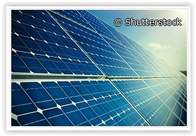
Disrupting the Solar Energy Status Quo
June 30, 2016 | CORDISEstimated reading time: 2 minutes
For decades, solar technology and applications have been dependent on dye-sensitised solar cells (DSSCs). To mimic nature’s absorption of light during photosynthesis, DSSCs use a photoactive dye that absorbs photons and uses their energy to excite electrons, which are then transferred into a nanocrystalline titanium dioxide layer. Although this process works well, the high-temperature processing required for titanium is not compatible with low-cost fabrication methods – an impediment to the mass market production of solar panels and thus a roadblock to increased use of solar energy.
Instead of being satisfied with the status quo, the EU-funded NANOMATCELL project decided to find a better way, and in doing so, will potentially provide a big boost to the solar energy industry.
Goodbye Titanium
NANOMATCELL researchers took aim at the use of titanium, with the intention of replacing it with innovative new materials and technologies for high-efficiency, solution processed solar cells. Bringing together experts from the fields of material science, chemistry, surface passivation and physics, the team set out to better harness the solar spectrum by inventing both new materials capable of yielding high-power conversion efficiency solar cells and novel panchromatic semiconductors based on environmentally friendly compounds and processes.
Achieving these objectives was no small feat as they required the development of a number of new strategies and components. For example, the team first had to develop new strategies for the synthesis, growth and doping of semiconductor nanocrystals and nanowires. As dye plays a central role in the function of DSSCs, researchers also had to create new dyes capable of taking full advantage of a larger portion of the spectrum – meaning new dyes for short wavelengths and new dyes for enhanced absorption in the near-infrared range had to be created.
Increased market uptake
But that’s just the DSSCs themselves, there was also the challenge of what to do with the light once it was absorbed. Here too researchers made significant developments in improving the overall efficiency of solar cells. In fact, the NANOMATCELL project produced a range of solar cells based on panchromatic inorganic and hybrid absorbers – all of which demonstrate enhanced performance and a potential to reach even further optimisation.
Thanks to the new processing methods developed by the project, ground-breaking efficiencies in excess of 15 % have been reached with some solar cells. In other words, NANOMATCELL advanced the state of DSSCs to such a level of efficiency that widespread market uptake looks likely.
Ongoing Impact
Although the project itself has ended, the impact of its work goes on. According to recently published research in the journal ‘Nature Communications’, a new hybrid photodetector incorporating both graphene and quantum dots is now in the works. The combination of these two material technologies could lead to fast, efficient and low-cost devices capable of detecting across the visible, near-infrared and short-wave (SWIR) spectral regions to a wavelength of around 3 µm.
Researchers believe this novel approach will be compatible with the high-volume silicon CMOS manufacturing process, as well as emerging flexible electronic platforms. As current high-efficiency photo-detection in the SWIR region beyond 1 µm tends to rely on relatively expensive devices, this development represents yet another disruption to the traditional approach to solar cell technology – with many cost-saving benefits to follow.
Share on:


Testimonial
"Our marketing partnership with I-Connect007 is already delivering. Just a day after our press release went live, we received a direct inquiry about our updated products!"
Rachael Temple - AlltematedSuggested Items
HyRel Technologies Showcases Summer Intern Success Through Hands-On Innovation
09/16/2025 | HyRel TechnologiesHyRel Technologies, a global provider of quick turn semiconductor modification solutions, proudly highlights the accomplishments of its two recent summer interns, Danny Hoang and Nisarg Jadav.
Automation Meets Sustainability
09/08/2025 | Rick Nichols, GreenSource EngineeringGreenSource Engineering (GSE) is proud to have contributed to the first successful reshoring of a PCB facility on a greenfield site in the United States. While we are honored to have played a key role, full credit for this achievement goes to SEL for its vision, commitment, and professionalism.
Japan’s OHISAMA Project Aims to Beam Solar Power from Space This Year
07/14/2025 | I-Connect007 Editorial TeamJapan could be on the cusp of making history with its OHISAMA project in its quest to become the first country to transmit solar power from space to Earth, The Volt reported.
Connect the Dots: The Future of PCB Design and Manufacturing
07/02/2025 | Matt Stevenson -- Column: Connect the DotsFor some time, I have been discussing the increasing complexity of PCBs and how designers can address the constantly evolving design requirements associated with them. My book, "The Printed Circuit Designer’s Guide to… Designing for Reality," details best practices for creating manufacturable boards in a modern production environment.
Project GENESIS Minimizes Ecological Footprint in Europe’s Semiconductor Industry
06/06/2025 | Fraunhofer IPMSA pan-European consortium dedicated to developing sustainable processes and technologies for the semiconductor-manufacturing supply chain announces the launch of the GENESIS project.