


 Standard of Excellence: The Future of Fabrication—From Art to Automation
 Knocking Down the Bone Pile: The Business Case for Component Reclamation
 Global Sourcing Spotlight: The Hidden Power of the Rep Network


To continue advancing, next-generation electronic devices must fully exploit the nanoscale, where materials span just billionths of a meter. But balancing complexity, precision, and manufacturing scalability on such fantastically small scales is inevitably difficult. Fortunately, some nanomaterials can be coaxed into snapping themselves into desired formations-a process called self-assembly.
Scientists at the U.S. Department of Energy's (DOE) Brookhaven National Laboratory have just developed a way to direct the self-assembly of multiple molecular patterns within a single material, producing new nanoscale architectures. The results were published in the journal Nature Communications.
"This is a significant conceptual leap in self-assembly," said Brookhaven Lab physicist Aaron Stein, lead author on the study. "In the past, we were limited to a single emergent pattern, but this technique breaks that barrier with relative ease. This is significant for basic research, certainly, but it could also change the way we design and manufacture electronics."
Microchips, for example, use meticulously patterned templates to produce the nanoscale structures that process and store information. Through self-assembly, however, these structures can spontaneously form without that exhaustive preliminary patterning. And now, self-assembly can generate multiple distinct patterns-greatly increasing the complexity of nanostructures that can be formed in a single step.
"This technique fits quite easily into existing microchip fabrication workflows," said study coauthor Kevin Yager, also a Brookhaven physicist. "It's exciting to make a fundamental discovery that could one day find its way into our computers."
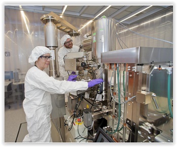
The experimental work was conducted entirely at Brookhaven Lab's Center for Functional Nanomaterials (CFN), a DOE Office of Science User Facility, leveraging in-house expertise and instrumentation.
Cooking up organized complexity
The collaboration used block copolymers-chains of two distinct molecules linked together-because of their intrinsic ability to self-assemble.
"As powerful as self-assembly is, we suspected that guiding the process would enhance it to create truly 'responsive' self-assembly," said study coauthor Greg Doerk of Brookhaven. "That's exactly where we pushed it."
To guide self-assembly, scientists create precise but simple substrate templates. Using a method called electron beam lithography-Stein's specialty-they etch patterns thousands of times thinner than a human hair on the template surface. They then add a solution containing a set of block copolymers onto the template, spin the substrate to create a thin coating, and "bake" it all in an oven to kick the molecules into formation. Thermal energy drives interaction between the block copolymers and the template, setting the final configuration-in this instance, parallel lines or dots in a grid.
"In conventional self-assembly, the final nanostructures follow the template's guiding lines, but are of a single pattern type," Stein said. "But that all just changed."
Lines and dots, living together
The collaboration had previously discovered that mixing together different block copolymers allowed multiple, co-existing line and dot nanostructures to form.
"We had discovered an exciting phenomenon, but couldn't select which morphology would emerge," Yager said. But then the team found that tweaking the substrate changed the structures that emerged. By simply adjusting the spacing and thickness of the lithographic line patterns-easy to fabricate using modern tools-the self-assembling blocks can be locally converted into ultra-thin lines, or high-density arrays of nano-dots.
"We realized that combining our self-assembling materials with nanofabricated guides gave us that elusive control. And, of course, these new geometries are achieved on an incredibly small scale," said Yager.
"In essence," said Stein, "we've created 'smart' templates for nanomaterial self-assembly. How far we can push the technique remains to be seen, but it opens some very promising pathways."
Gwen Wright, another CFN coauthor, added, "Many nano-fabrication labs should be able to do this tomorrow with their in-house tools-the trick was discovering it was even possible."
The scientists plan to increase the sophistication of the process, using more complex materials in order to move toward more device-like architectures.
"The ongoing and open collaboration within the CFN made this possible," said Charles Black, director of the CFN. "We had experts in self-assembly, electron beam lithography, and even electron microscopy to characterize the materials, all under one roof, all pushing the limits of nanoscience."


