


 It’s Only Common Sense: Marketing Isn’t Fluff, It’s Ammunition
 Driving Innovation: Mechanical and Optical Processes During Rigid-flex Production
 The Chemical Connection: Onshoring PCB Production—Daunting but Certainly Possible


Ventec International Expands USA Manufacturing Capacity With Investment in New Equipment
January 30, 2017 | VentecEstimated reading time: 1 minute
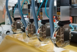
Ventec International Group has increased the manufacturing capacity at its Chicago facility (700 Lee Street, Elk Grove Village, IL) with major investment into new state-of-the-art equipment for laminate/prepregs as well as its newest ranges of PCB base-materials including complementary products such as flex and rigid-flex circuit board materials, back-up, entry and routing materials, foils and coatings.
To capture growth opportunities in prepreg markets, which are driven by particular demand from high reliability, military and aerospace applications, a Pasquato TE 15 prepreg slitter/sheeter from Italy has been installed. At the same time, cooler storage capacity has been doubled and provides ‘storage 1’ conditions of below 5oC for prepreg materials. Prepreg vacuum sealing capacity has also been doubled with the addition of a dedicated vacuum packer.
For cut-to-size back-up and entry materials, further cutting capacity is provided through the addition of a Kitagawa diamond blade saw alongside the existing Yow Shi diamond blade saw for laminate. Two Excellon Mark V Driller/Router Machines - one for tooling prepreg and one for tooling back-up and entry - have been added alongside the existing Excellon IV drill machine, adding drilling capacity to allow for materials to be supplied with tooling holes where required. Having two saws, additional drilling capability, a new shrink wrap packaging machine dedicated to packaging back-up and entry materials as well as a second delivery vehicle all in one location, offers customers a unique advantage through fast turn-around and quick-delivery material sourcing.
Jack Pattie, President of Ventec's US operation commented, "Ventec is continuing its phased and strategic investment plan across our global network of service centers. This latest investment in our Chicago facility enables our US customers to enjoy one single quick-turn access point to an extraordinary portfolio of prepregs and complementary products & services today."
About Ventec International
With volume manufacturing facilities and HQ in Suzhou China, Ventec International specializes in advanced copper clad glass reinforced and metal backed substrates for the PCB industry. With distribution locations and quick-turn CCL manufacturing sites in both the US and Europe, Ventec International is a premier supplier to the Global PCB industry. For more information, click here.
Share on:


Testimonial
"Our marketing partnership with I-Connect007 is already delivering. Just a day after our press release went live, we received a direct inquiry about our updated products!"
Rachael Temple - AlltematedSuggested Items
WestDev Announces Advanced Thermal Analysis Integration for Pulsonix PCB Design Suite
10/29/2025 | WestDev Ltd.Pulsonix, the industry-leading PCB design software from WestDev Ltd., announced a major enhancement to its design ecosystem: a direct interface between Pulsonix and ADAM Research's TRM (Thermal Risk Management) analysis software.
Designers Notebook: Power and Ground Distribution Basics
10/29/2025 | Vern Solberg -- Column: Designer's NotebookThe principal objectives to be established during the planning stage are to define the interrelationship between all component elements and confirm that there is sufficient surface area for placement, the space needed to ensure efficient circuit interconnect, and to accommodate adequate power and ground distribution.
Episode 6 of Ultra HDI Podcast Series Explores Copper-filled Microvias in Advanced PCB Design and Fabrication
10/15/2025 | I-Connect007I-Connect007 has released Episode 6 of its acclaimed On the Line with... American Standard Circuits: Ultra High Density Interconnect (UHDI) podcast series. In this episode, “Copper Filling of Vias,” host Nolan Johnson once again welcomes John Johnson, Director of Quality and Advanced Technology at American Standard Circuits, for a deep dive into the pros and cons of copper plating microvias—from both the fabricator’s and designer’s perspectives.
Nolan’s Notes: Tariffs, Technologies, and Optimization
10/01/2025 | Nolan Johnson -- Column: Nolan's NotesLast month, SMT007 Magazine spotlighted India, and boy, did we pick a good time to do so. Tariff and trade news involving India was breaking like a storm surge. The U.S. tariffs shifted India from one of the most favorable trade agreements to the least favorable. Electronics continue to be exempt for the time being, but lest you think that we’re free and clear because we manufacture electronics, steel and aluminum are specifically called out at the 50% tariff levels.
MacDermid Alpha & Graphic PLC Lead UK’s First Horizontal Electroless Copper Installation
09/30/2025 | MacDermid Alpha & Graphic PLCMacDermid Alpha Electronics Solutions, a leading supplier of integrated materials and chemistries to the electronics industry, is proud to support Graphic PLC, a Somacis company, with the installation of the first horizontal electroless copper metallization process in the UK.