


 Driving Innovation: Mechanical and Optical Processes During Rigid-flex Production
 It’s Only Common Sense: Your Biggest Competitor Is Complacency
 The Chemical Connection: Onshoring PCB Production—Daunting but Certainly Possible


Laser Patterning & Metallization to Reduce Process Steps for PCB Manufacturing
August 29, 2017 | Joel Schrauben, Cameron Tribe, Christopher Ryder and Jan Kleinert, ELECTRO SCIENTIFIC INDUSTRIESEstimated reading time: 1 minute
Abstract
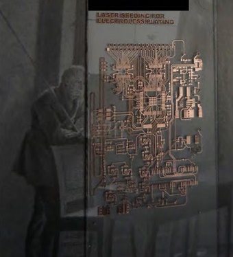
Glass offers a number of advantages as a dielectric material, such as a low coefficient of thermal expansion (CTE), high dimensional stability, high thermal conductivity and suitable dielectric constant. These properties make glass an ideal candidate for, among other things, package substrate and high-frequency PCB applications. We report here a novel process for the production of printed circuit boards and integrated circuit packaging using glass as both a dielectric medium and a platform for wiring simultaneously.
An ultrafast laser is used to etch away the desired pattern (pads, wires and vias) in the glass, and copper plating is “seeded” through the laser-based deposition of copper droplets. The seeded area is then plated using electroless plating followed by electroplating. Demonstrations of fine pitch wires, variable diameter through holes and blind vias, and a multilayer stack are shown. The deposits have a resistivity less than a factor of 1.5x that of bulk copper for 5-10 mm wires. Plated lines in borosilicate glass of 7-10 μm width and 5-20 μm depth and line spacing down to ~10 μm are demonstrated, as well as vias with a top diameter approaching 100 μm for 150 μm glass and 40 μm for 50 μm glass.
The process presents the potential for significant material savings in terms of base materials, process chemicals, and waste disposal/recycling costs (glass is on the order of 100-fold less expensive than some current high-frequency dielectrics, and wet processes account for a large part of standard PCB/substrate manufacturing). Additionally, the processes are amenable toward other dielectric materials such as FR-4, polyimide and PTFE-based materials.
Introduction
Increased demand for high data transmission rates is driving the development of smaller PCB features. Electrical circuits are reaching the physical limitations of traditional PCB dielectric materials under which electromagnetic compatibility can be controlled.
To read the full version of this article which appeared in the August 2017 issue of The PCB Magazine, click here.
Share on:


Testimonial
"Advertising in PCB007 Magazine has been a great way to showcase our bare board testers to the right audience. The I-Connect007 team makes the process smooth and professional. We’re proud to be featured in such a trusted publication."
Klaus Koziol - atgSuggested Items
WestDev Announces Advanced Thermal Analysis Integration for Pulsonix PCB Design Suite
10/29/2025 | WestDev Ltd.Pulsonix, the industry-leading PCB design software from WestDev Ltd., announced a major enhancement to its design ecosystem: a direct interface between Pulsonix and ADAM Research's TRM (Thermal Risk Management) analysis software.
Designers Notebook: Power and Ground Distribution Basics
10/29/2025 | Vern Solberg -- Column: Designer's NotebookThe principal objectives to be established during the planning stage are to define the interrelationship between all component elements and confirm that there is sufficient surface area for placement, the space needed to ensure efficient circuit interconnect, and to accommodate adequate power and ground distribution.
Episode 6 of Ultra HDI Podcast Series Explores Copper-filled Microvias in Advanced PCB Design and Fabrication
10/15/2025 | I-Connect007I-Connect007 has released Episode 6 of its acclaimed On the Line with... American Standard Circuits: Ultra High Density Interconnect (UHDI) podcast series. In this episode, “Copper Filling of Vias,” host Nolan Johnson once again welcomes John Johnson, Director of Quality and Advanced Technology at American Standard Circuits, for a deep dive into the pros and cons of copper plating microvias—from both the fabricator’s and designer’s perspectives.
Nolan’s Notes: Tariffs, Technologies, and Optimization
10/01/2025 | Nolan Johnson -- Column: Nolan's NotesLast month, SMT007 Magazine spotlighted India, and boy, did we pick a good time to do so. Tariff and trade news involving India was breaking like a storm surge. The U.S. tariffs shifted India from one of the most favorable trade agreements to the least favorable. Electronics continue to be exempt for the time being, but lest you think that we’re free and clear because we manufacture electronics, steel and aluminum are specifically called out at the 50% tariff levels.
MacDermid Alpha & Graphic PLC Lead UK’s First Horizontal Electroless Copper Installation
09/30/2025 | MacDermid Alpha & Graphic PLCMacDermid Alpha Electronics Solutions, a leading supplier of integrated materials and chemistries to the electronics industry, is proud to support Graphic PLC, a Somacis company, with the installation of the first horizontal electroless copper metallization process in the UK.