


 It’s Only Common Sense: The Phone Is Still Mightier Than the Keyboard
 The Marketing Minute: Marketing With Layers


Nanocarbon Materials Are Challenging Silicon – From Transparent Electronics to Bendable 3D Displays
September 7, 2017 | Aalto UniversityEstimated reading time: 3 minutes
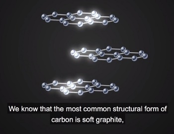
The superior characteristics of nanocarbon make it an extremely promising material for numerous current and future applications.
"Light and flexible nanocarbon materials conduct electricity better than copper and have greater mechanical strength than steel. They are also good thermal conductors and have great potential for use in reinforced composites, nanoelectronics, sensors and nanomechanical devices," says professor Esko I. Kauppinen, the director of Aalto University’s NanoMaterials research group.
Recently, significant advances have been made in the development of nanocarbon materials and their applications. The International Symposium on Nanocarbon Materials gathered the world’s cutting-edge nanocarbon material researchers to Aalto University.
Flexible and transparent electronics
One of the breakthrough applications of carbon nanotubes (CNT) is foreseen in transistor technology. Carbon nanotubes have already been shown to outperform silicon as the semiconducting material for transistors.
"The structure of CNT makes it more chemically stable than silicon. Compared to silicon CMOS technology, carbon nanotube devices are about 5-10 times faster, over 10 times more efficient in power consumption and much smaller in size," says professor Lian-Mao Peng from Peking University.
There are still several technical problems to solve before CNT based chips become commercial products; the main concerns are the material’s thermal and long-term stability. Also, the silicon industry is very mature and it will take major efforts to replace silicon as semiconducting material in electronics.
"I would say in 3-5 years we will see CNTs in some low-end applications that are not dominated by silicon, like flexible and transparent electronics. Maybe in 10-15 years CNT will get to mainstream semiconductor industry with high performance and low power consumption," Peng says.
Carbon nanotube films are also a potential material for the charge selection/conduction layer of perovskite solar cells. Perovskite solar cells challenge the traditional silicon cells with a cheaper, simpler and more energy-efficient manufacturing process.
"The best reported perovskite solar cells have the power conversion efficiency of 22 percent which is compatible to silicon solar cells. And, they can be much cheaper than silicon cells as organic solar cells. Also, flexible and transparent perovskite solar cells could be integrated in windows and other building surfaces. I expect they could become commercial in 3-5 years," says professor Shigeo Maruyama from the University of Tokyo.
Carbon nanostructure such as graphene gets exciting new applications through nanoscale technologies. Photo: Alexander Savin.
Shaping surfaces with curved and 3D formed displays
Besides carbon nanotubes, nanocarbons are found in various structures like spherical fullerens and single atomic layer graphene. In 2006, a new carbon composite nanomaterial was discovered by Aalto University NanoMaterials Group headed by professor Kauppinen. The material was named and patented as NanoBud.
"NanoBuds are formed by binding spheroidal carbon molecules, fullerenes, to the outer sidewalls of single-walled carbon nanotubes. Printed on a thin film of plastic, NanoBuds can be used in touch screens of mobile phones, cameras and wearable devices," Kauppinen says.
The discovery of NanoBud led to the establishment of Canatu Oy to develop and exploit commercial innovations. The Aalto University spin-off company manufactures 3D formable, flexible and transparent carbon NanoBud films and touch sensors for consumer electronics and automotive industry.
The NanoMaterials Group is one of the world's leading gas-phase synthesis laboratories for NanoBuds, nanotubes and nanomaterials. In Aalto University, high-level nanocarbon material research is conducted also in several other research teams in the School of Science, School of Chemical Engineering and School of Electrical Engineering.
"Besides our strong international networks, nanocarbon material research collaboration within Aalto University is most fruitful. By learning from each other we can achieve much better results compared to what we could accomplish ourselves," Kauppinen says.
The future of nanocarbon materials shines bright.
Share on:


Testimonial
"We’re proud to call I-Connect007 a trusted partner. Their innovative approach and industry insight made our podcast collaboration a success by connecting us with the right audience and delivering real results."
Julia McCaffrey - NCAB GroupSuggested Items
Episode 6 of Ultra HDI Podcast Series Explores Copper-filled Microvias in Advanced PCB Design and Fabrication
10/15/2025 | I-Connect007I-Connect007 has released Episode 6 of its acclaimed On the Line with... American Standard Circuits: Ultra High Density Interconnect (UHDI) podcast series. In this episode, “Copper Filling of Vias,” host Nolan Johnson once again welcomes John Johnson, Director of Quality and Advanced Technology at American Standard Circuits, for a deep dive into the pros and cons of copper plating microvias—from both the fabricator’s and designer’s perspectives.
Nolan’s Notes: Tariffs, Technologies, and Optimization
10/01/2025 | Nolan Johnson -- Column: Nolan's NotesLast month, SMT007 Magazine spotlighted India, and boy, did we pick a good time to do so. Tariff and trade news involving India was breaking like a storm surge. The U.S. tariffs shifted India from one of the most favorable trade agreements to the least favorable. Electronics continue to be exempt for the time being, but lest you think that we’re free and clear because we manufacture electronics, steel and aluminum are specifically called out at the 50% tariff levels.
MacDermid Alpha & Graphic PLC Lead UK’s First Horizontal Electroless Copper Installation
09/30/2025 | MacDermid Alpha & Graphic PLCMacDermid Alpha Electronics Solutions, a leading supplier of integrated materials and chemistries to the electronics industry, is proud to support Graphic PLC, a Somacis company, with the installation of the first horizontal electroless copper metallization process in the UK.
Electrodeposited Copper Foils Market to Grow by $11.7 Billion Over 2025-2032
09/18/2025 | Globe NewswireThe global electrodeposited copper foils market is poised for dynamic growth, driven by the rising adoption in advanced electronics and renewable energy storage solutions.
MacDermid Alpha Showcases Advanced Interconnect Solutions at PCIM Asia 2025
09/18/2025 | MacDermid Alpha Electronics SolutionsMacDermid Alpha Electronic Solutions, a global leader in materials for power electronics and semiconductor assembly, will showcase its latest interconnect innovations in electronic interconnect materials at PCIM Asia 2025, held from September 24 to 26 at the Shanghai New International Expo Centre, Booth N5-E30