


 Driving Innovation: Mechanical and Optical Processes During Rigid-flex Production
 It’s Only Common Sense: Your Biggest Competitor Is Complacency
 The Chemical Connection: Onshoring PCB Production—Daunting but Certainly Possible


Metal Printing Offers Low-Cost Way to Make Flexible, Stretchable Electronics
December 29, 2017 | North Carolina State UniversityEstimated reading time: 1 minute
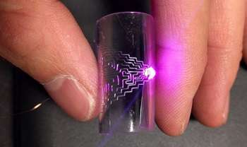
Researchers from North Carolina State University have developed a new technique for directly printing metal circuits, creating flexible, stretchable electronics. The technique can use multiple metals and substrates and is compatible with existing manufacturing systems that employ direct printing technologies.
“Flexible electronics hold promise for use in many fields, but there are significant manufacturing costs involved – which poses a challenge in making them practical for commercial use,” says Jingyan Dong, corresponding author of a paper on the work and an associate professor in NC State’s Edward P. Fitts Department of Industrial & Systems Engineering.
“Our approach should reduce cost and offer an efficient means of producing circuits with high resolution, making them viable for integrating into commercial devices,” Dong says.
The technique uses existing electrohydrodynamic printing technology, which is already used in many manufacturing processes that use functional inks. But instead of ink, Dong’s team uses molten metal alloys with melting points as low as 60 degrees Celsius. The researchers have demonstrated their technique using three different alloys, printing on four different substrates: one glass, one paper and two stretchable polymers.
“This is direct printing,” Dong says. “There is no mask, no etching and no molds, making the process much more straightforward.”
The researchers tested the resilience of the circuits on a polymer substrate and found that the circuit’s conductivity was unaffected even after being bent 1,000 times. The circuits were still electrically stable even when stretched to 70 percent of tensile strain.
The researchers also found that the circuits are capable of “healing” themselves if they are broken by being bent or stretched too far.
“Because of the low melting point, you can simply heat the affected area up to around 70 degrees Celsius and the metal flows back together, repairing the relevant damage,” Dong says.
The researchers demonstrated the functionality of the printing technique by creating a high-density touch sensor, fitting a 400-pixel array into one square centimeter.
“We’ve demonstrated the resilience and functionality of our approach, and we’re open to working with the industry sector to implement the technique in manufacturing wearable sensors or other electronic devices,” Dong says.
Share on:


Testimonial
"We’re proud to call I-Connect007 a trusted partner. Their innovative approach and industry insight made our podcast collaboration a success by connecting us with the right audience and delivering real results."
Julia McCaffrey - NCAB GroupSuggested Items
Henger Microelectronics Expands Global Footprint with Major Equipment Shipment to Southeast Asia
10/31/2025 |Henger Microelectronics has reached a major milestone in its global expansion strategy with the successful shipment of advanced plasma etching and cleaning systems, along with automation equipment, to multiple countries and regions across Southeast Asia. This achievement marks a significant step forward in the company’s international growth and reinforces its position as a leading force in the global plasma equipment industry.
PCBAA Names Industry Veteran Dan Weber to Board of Directors
10/31/2025 | PCBAAThe Printed Circuit Board Association of America has added Dan Weber, Executive Vice President and General Counsel at TTM Technologies, to the PCBAA board of directors.
KLA Reports Fiscal Q1 2026 Results
10/31/2025 | PRNewswireKLA Corporation announced financial and operating results for its first quarter of fiscal year 2026, which ended on Sept. 30, 2025, and reported GAAP net income of $1.12 billion and GAAP net income per diluted share of $8.47 on revenues of $3.21 billion.
Samsung Teams With NVIDIA to Lead the Transformation of Global Intelligent Manufacturing Through New AI Megafactory
10/31/2025 | SamsungSamsung Electronics today announced plans to create a new AI Megafactory in collaboration with NVIDIA, marking a major milestone in the company’s efforts to lead the global paradigm shift toward AI-driven manufacturing.
Fresh PCB Concepts: Resilience and Renewal in Domestic PCB Manufacturing
10/30/2025 | Team NCAB -- Column: Fresh PCB ConceptsAs veterans of PCB manufacturing, we have spent much of our careers walking factory floors, examining copper circuits under microscopes, and troubleshooting plating lines when they go awry at 2 a.m. We can say with confidence that PCBs are the unsung heroes of modern life. They’re in everything, from toothbrushes and thermostats to satellites and defense systems.