


 Standard of Excellence: Building Intelligent Supply Chain Ecosystems Before Your Competitors Do
 SMT Perspectives & Prospects: The Architecture of Winston Churchill’s Leadership
 Global Sourcing Spotlight: Making Global Sourcing Simple Again


The speed of change in the electronics industry is rapidly accelerating. The direction in which the industry moves is constantly shifting and it needs participation, see you in San Diego. JTAG Technologies is excited to showcase here in San Diego the latest version of its acclaimed Visualizer graphical viewing tool for board (PCB) layouts and schematics. Allowing users to assess fault coverage data and pin-point production test faults in a snap.
Wide-ranging CAD support
With its wide range of CAD (EDA) tool import filters Visualizer is the number one choice for professional boundary-scan development and test engineers. Users can import schematic data direct from Mentor (Pads, DxDesigner, Capture) Cadence, Altium and Zuken tools as well as board layout information in ODB++ and a dozen other vendor specific formats.
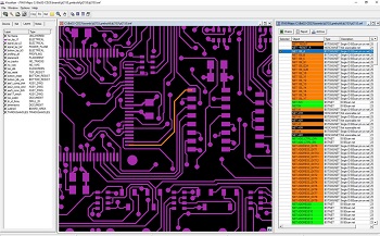
JTAG Maps
Introduced in this version of Visualizer, the new Maps feature offers a basic test-accessibility view by a simple click of the mouse. The view can easily be fine-tuned by adding just a few key component descriptions to a look up table. What’s more using customisable colors to indicate test coverage levels or access types, a color-coded schematic can be displayed or printed. Once the design has been optimized for boundary-scan test coverage and committed to layout, final application development can begin in the JTAG ProVision developer tool.
Additional new features
Visualize on (Test) Fail -When running a test sequence or during test debug within ProVision it is now possible to view all failing circuit nets on a schematic view, a layout view or both – automatically. This feature is ideal for small-scale production systems where the test operator is also responsible for fault diagnosis and rework.
Locate Next – during fault-finding the ‘locate next’ feature allows the user to track the course of a net connection through the layers of a PCB layout or the sheets of a schematic.
Multiple Color Themes - users can now define multiple color themes for distinguishing different net classifications e.g. for percentage fault coverage in schematics or fault nets in layouts to aid in debug and repair
View through layers - a highlighted fault net, perhaps as a result of a detected board connection fault, can now be viewed along its entire path and as it changes course through the board (pcb) layers.
Add notes – A note can be added anywhere at a fixed position on the schematic or layout. Ideal for conveying additional information about test processes or passing design details back and forth between users.
Peter van den Eijnden, MD JTAG Technologies, comments ‘ Our impressive enhancements to Visualizer come as a result of our commitments to customer liaison and also our work with various 3rd parties such as the EDA vendors’.
Another JTAG Highlight at APEX 2018 - ATE Integration: Simple and effective improvement of test coverage
Clients need to improve the overall test coverage of their assembled boards. It’s easy. Clients can simply combine their JTAG Technologies boundary-scan tools with todays’ existing automatic test equipment (ATE). JTAG works with any vendor of in-circuit testers (ICT), flying probes (FPT) or functional testers (FT).
ATE integration is completely trouble free and merely involves adapting execution software to operate in the specific ATE environment. In many cases we at JTAG develop dedicated, customized versions of the boundary-scan controllers or pods. This simplifies mechanical integration and preserves signal integrity.
Our experts will discuss the level of integration variation according to your needs.
About JTAG Technologies
JTAG Technologies is a market leader and technology innovator of boundary-scan software and hardware products and services. The company was the first to bring to the market such important advances as automated test generation, automated fault coverage analysis, automated flash and PLD programming via boundary-scan, and visualized boundary-scan analysis. Its customers include world leaders in electronics design and manufacturing such as Bae, Ericsson, Flextronics, Honeywell, Medtronic, Motorola, Philips, Raytheon, Rockwell-Collins, Samsung, and Sony. Its innovative boundary-scan products provide test preparation, test execution, test result analysis and in-system programming applications. With an installed base of over 9000 systems worldwide, JTAG Technologies serves the communications, medical electronics, avionics, defence, automotive, and consumer industries with offices throughout North America, Europe and Asia. JTAG Technologies headquarters are located in Eindhoven, The Netherlands. For more information, click here.


