


 Beyond the Board: How a Diminished Supplier Base Affects Complex PCB Manufacturing Readiness in Defense
 Defense Speak Interpreted: Hypersonics Report Back After Six Years of Silence
 American Made Advocacy: American Microelectronics Power the Future of High Technology


Ventec Passes AS9100 Revision D Transition Audit in China and UK
January 17, 2018 | Ventec International GroupEstimated reading time: 1 minute
Ventec International Group is pleased to announce that the company headquarters in Suzhou, China and its European headquarters in the United Kingdom have both successfully passed the transition audit to AS9100 Revision D with zero non-conformances in accordance with the Aerospace Supplier Quality System Certification Scheme. SGS, the world's leading inspection, verification, testing and certification company have received recommendation to issue the upgrade certification to AS9100 Revision D for both locations.
With the transition audit passes to AS9100 Revision D at Ventec’s China and UK facilities, OEMs and PCB fabrication customers servicing the aviation, space and defense industries can continue to rely on Ventec's fully accredited supply chain for high reliability laminates and prepregs. From manufacture through fabrication and global delivery, Ventec's high quality product portfolio of polyimides, high reliability FR-4, tec-speed range of high speed/low loss materials and tec-thermal range of IMS materials are all covered by the accreditation.
Mark Goodwin, COO commented: “Achieving highest supply chain standards is paramount to our successful growth and I’m delighted with our recent successful re-certification audits in China and the UK. The results reflect the hard work of our entire team in implementing and practicing the highest levels of quality throughout our supply chain, enabling our PCB and OEM customers to engage Ventec as a strategic partner in their safety critical supply chains, based not just on the proven performance of our materials but on our commitment to managing delivered quality to the highest standards.”
About Ventec International
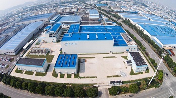
With volume manufacturing facilities and HQ in Suzhou China, Ventec International specializes in advanced copper clad glass reinforced and metal backed substrates for the PCB industry. With distribution locations and manufacturing sites in both the US and Europe, Ventec International is a premier supplier to the Global PCB industry. For more information, click here.
Share on:


Testimonial
"Advertising in PCB007 Magazine has been a great way to showcase our bare board testers to the right audience. The I-Connect007 team makes the process smooth and professional. We’re proud to be featured in such a trusted publication."
Klaus Koziol - atgSuggested Items
Nortech Systems Launches Power over Fiber Technology Platform for EMI-Sensitive Applications
04/08/2026 | Globe NewswireNortech Systems Incorporated, a leading provider of design and manufacturing solutions for complex electromedical devices and electromechanical systems, has announced the launch of its Power over Fiber technology platform.
Flexible Thinking: Designing Flex Circuits for Dynamic Reliability
04/09/2026 | Joe Fjelstad -- Column: Flexible ThinkingFlex circuits flex. No surprises there. However, they are also very commonly designed into products because they are thin and offer consistent thickness and dielectric properties, attributes highly prized by present-day product designers of personal electronics. This would include smartphones and, increasingly, wearable electronics for medical monitoring and even fashion.
Understanding Tolerances in Flexible Circuit Design
04/01/2026 | Chris Clark, Flexible Circuit TechnologiesThe challenge with cumulative tolerances is meeting the dimensional requirements for items dimensioned on a drawing or specification for a flexible or rigid-flex circuit. It is critical to understand the fabrication processes and how features are defined when creating your tolerance requirements.
Target Condition: An Exploration of Flooding PCB Layers
04/02/2026 | Kelly Dack -- Column: Target ConditionThe concept of flooding PCB layers with copper has been around for so long, you’d think we’d have it mastered. We haven’t. (Oh, and by “we,” I mean design engineers and the software tools we depend on.) Years ago, PCB artwork was created by hand using light tables, with tape applied to Mylar. Signals were slow, traces were relatively wide, and high-current paths were simply “beefed up” with wider copper. Signal integrity wasn’t yet a driving concern. Today, solid return paths are fundamental to robust design. We understand the importance of continuous reference planes for signal integrity and EMI control.
New, Greener Solutions for Etch: Novel Copper Extraction
03/30/2026 | Richard Nichols, GreenSource Engineering“Novel” is a typical marketing phrase that implies new and unique, but often “novel” actually means an established technology being applied to a new field or application. This, in turn, is often driven by newly relevant external motivation. GreenSource has been working on just such a solution: novel copper extraction, offering a better and greener alternative to traditional LLE control systems for cupric chloride etch.