


 Dan’s Biz Bookshelf: Four Important Books You Need to Read (Not Just Say You Have)
 Marcy’s Musings: Advancing the Advanced Materials Discussion
 The Marketing Minute: Cracking the Code of Technical Marketing


Equipment/Process Selection: Case Study of a DMADV Approach to PCB FAB Process Design
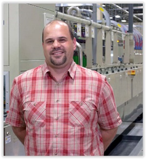
February 5, 2018 | Alex Stepinski, WHELEN ENGINEERINGEstimated reading time: 1 minute
Background
In 2014, Whelen Engineering Company, the OEM market leader in the emergency warning industry, developed the world’s first green smart PCB fab factory as a captive operation servicing internal demand. Due to the success of this venture, in 2016, a decision was made to explore building an upgraded factory which would serve the merchant market. This article outlines the approach we took to designing this new phase of our commercial existence, which has now been spun off as a separate business unit known as Greensource Fabrication. This new business unit is expected to go live in 2018.
Summary Approach
In our experience, a holistic DMADV approach to complex process design is not commonly used in the PCB industry. This approach requires a commitment to dedicated R&D re-sources, extensive travel by the technical team, a great deal of hands-on experience, as well as significant investment capital. Since very few PCB fabs perform R&D, we believe that there is a currently a very high ROI to this approach with low risk, since it is easy to design and secure strong competitive advantages when everyone else is just copying each other.
To read the full version of this article which appeared in the January 2018 issue of The PCB007 Magazine, click here.
Share on:


Testimonial
"The I-Connect007 team is outstanding—kind, responsive, and a true marketing partner. Their design team created fresh, eye-catching ads, and their editorial support polished our content to let our brand shine. Thank you all! "
Sweeney Ng - CEE PCBSuggested Items
Accelerating Embedded Innovation: Orthogone Becomes Texas Instruments Design Partner
09/17/2025 | PRNewswireOrthogone Technologies Inc., a leader in advanced embedded systems and FPGA development, is proud to announce its official designation as a Texas Instruments (TI) Design Services Partner.
BLT Joins Microchip Partner Program as Design Partner
09/17/2025 | BUSINESS WIREBLT, a U.S.-owned and operated engineering design services firm announced it has joined the Microchip Design Partner Program.
Staying on Top of Signal Integrity Challenges
09/16/2025 | Andy Shaughnessy, Design007 MagazineOver the years, Kris Moyer has taught a variety of advanced PCB design classes, both online IPC courses and in-person classes at California State University-Sacramento, where he earned his degrees in electrical engineering. Much of his advanced curriculum focuses on signal integrity, so we asked Kris to discuss the trends he’s seeing in signal integrity today, the SI challenges facing PCB designers, and his go-to techniques for controlling or completely eliminating SI problems.
American Standard Circuits to Exhibit and Host Lunch & Learn at PCB West 2025
09/17/2025 | American Standard CircuitsAnaya Vardya, President, and CEO of American Standard Circuits/ASC Sunstone Circuits has announced that his company will once again be exhibiting at PCB West 2025 to be held at the Santa Clara Convention Center on Wednesday, October 1, 2025.
ASM Technologies Limited signs MoU with the Guidance, Government of Tamilnadu to Expand Design-Led Manufacturing capabilities for ESDM
09/15/2025 | ASM TechnologiesASM Technologies Limited, a pioneer in Design- Led Manufacturing in the semiconductor and automotive industries, announced signing of Memorandum of Understanding (MoU) with the Guidance, Government of Tamilnadu whereby it will invest Rs. 250 crores in the state to expand its ESDM related Design-Led Manufacturing and precision engineering capacity. ASM Technologies will acquire 5 acres of land from the Government of Tamilnadu to set up a state-of-the-art design facility in Tamil Nadu's growing technology manufacturing ecosystem, providing a strong strategic advantage and long-term benefits for ASM.