


 Dan’s Biz Bookshelf: ‘Growth Hacker Marketing’
 Happy’s Tech Talk #38: Novel Metallization for UHDI
 It’s Only Common Sense Mastering the Follow-Up—The Key to Closing More Deals


Multi-board Design with Altium’s Ben Jordan
July 25, 2018 | I-Connect007 Editorial TeamEstimated reading time: 5 minutes
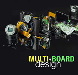
Not too long ago, historically speaking, most electronic products contained only one PCB. But multi-board designs have become almost ubiquitous over the past decade, and EDA software companies are working to improve and simplify the multi-board design process. For the June 2018 issue of Design007 Magazine, Editors Andy Shaughnessy and Stephen Las Marias spoke with Ben Jordan, director of product and persona marketing for Altium, about the company’s multi-board design tools, the challenges that customers face, and the numerous trade-offs that designers must contend with while performing multi-board design.
Andy Shaughnessy: Ben, why don’t you begin by telling us about multi-board design and multi-board EDA tools.
Ben Jordan: Multi-board design is, from my and Altium's point of view, simply the challenge of designing systems where there is more than one printed circuit board. It's not a complicated concept, and many of Altium's engineers and product managers have come from a background of designing new electronics. We even had our own internal hardware team for some time, doing the FPGA development boards. So we had some pretty high-end designers, people like Dave Jones, who runs the EEV blog now, and some of his colleagues back in Australia. We also had the team in Shanghai for a while doing IoT modular design. This all ended up being multi-board systems design.
One reason engineering firms do multi-board designs is to divide and conquer. We want to partition a bigger product into smaller modules to make the task of designing those modules and testing those modules as individual clusters of functions that sort of make sense together. You have the upside of being able to properly test and measure, and control supply chain issues, and design for fabrication and assembly if you have the ability of breaking up a large, complex product into small replaceable units.
This is not just for electronics; this is not a new concept. It's done in every other industry. We know that just about every professional PCB designer at some point is going to be designing a board, if they are not already, that's just one board in a larger system, and they may be involved in designing a larger system and integrating those modules. It makes sense that a mainstream professional development tool should have multiboard capabilities and shouldn't be considered a high-end feature.
It took a while because it required a new 3D modeling engine for doing 3D properly and efficiently; bringing multiple large complex PCB designs into a single editor workspace requires a lot of memory and computing power, otherwise the whole thing becomes unusable. So that was a big challenge for us, and it took some time, but we've finally been able to release that for Altium Designer 18.
We took the company into IoT experimentation in Shanghai. We’ve implemented stamp-based form-factor modules, and we were doing our FPGA development boards, the NanoBoard NB1, the NanoBoard 2, and NanoBoard 3000, which were all multi-board modular systems tems that could reconfigure the platform. We encountered all the challenges that people have with manufacturing boards of different layer stacks, but how do you optimize that? Is there a way the tools can offer you a way of analyzing and checking layer stack compatibility, so you can consolidate and make the best use of panel space fabrication?
Shaughnessy: What are some of the challenges designers typically face in multi-board design?
Jordan: One that is a real pain in the derriere is connectivity management.
Connectivity management is a big piece of the problem, because it’s so common for a component library in the CAD tool to look at the 3D model and the footprint (or decal or pattern, depending on what CAD tool you come from) with the mating face top down. The footprint for the connectors that you are using traditionally has them all numbered starting at the top left, anti-clockwise. In other words, you have a plug and you have a socket, and when the receptacle is reversed on the bottom side of one of the modules, because it’s got it sandwiched down on the baseboard, your pin numbering is mirrored, and it’s a problem. These cause headaches with managing pinouts. Then there’s the other side of it where you want to be able to swap some things around to optimize the layout and routing on one of the modules, and you need to be able to propagate changes like that throughout the broader system. So, connectivity management should be a part of pin-swapping as well.
Looking into the future, we’ve solved the basic pin assignments, connectivity management, and synchronization of pin swaps on the schematic side. What we have not yet done, but it’s on our road map, is model the cables. There’s a multi-board assembly and there’s cable connectivity between them. Maybe a single wire or a multi-point cable or a harness. We don’t compete with the MCAD tools which do a fabulous job of modeling cable harness assemblies, and it’s not in our plan to try to do what they do; SolidWorks Electrical is fantas-tic. But the goal is to model wire and cable to a level where a PCB designer can actually make sure they are specifying the basics of it, saying this goes to here and here and joins these boards together, and it has to sit in this kind of envelope in 3D, and it’s got these connections, and these signals travel through it, and we can swap pins again.
There’s a lot more we could do in this space, in this domain with problem solving, I think. We haven’t done anything with power integrity or signal integrity, for example. But that is definitely something that has to be considered with multi-board design. Speaking of power integrity, it’s very easy to forget that you have one PCB and if you test that one PCB, it will pass EMI requirements in isolation. You make that a part of a multi-board system where there are signals going across connectors and return paths may be forced around the design through power cables in strange ways, if you can’t design your connectivity right.
Individual modules may well pass for FCC regulations or CE regulations, and then completely fail once you integrate the whole sys-tem together as a multi-board assembly. So, these are the kinds of issues we have to think about.
To read this entire interview, which appeared in the June 2018 issue of Design007 Magazine, click here.
Share on:


Suggested Items
RF PCB Design Tips and Tricks
05/08/2025 | Cherie Litson, EPTAC MIT CID/CID+There are many great books, videos, and information online about designing PCBs for RF circuits. A few of my favorite RF sources are Hans Rosenberg, Stephen Chavez, and Rick Hartley, but there are many more. These PCB design engineers have a very good perspective on what it takes to take an RF design from schematic concept to PCB layout.
Cadence Unveils Millennium M2000 Supercomputer with NVIDIA Blackwell Systems
05/08/2025 | Cadence Design SystemsAt its annual flagship user event, CadenceLIVE Silicon Valley 2025, Cadence announced a major expansion of its Cadence® Millennium™ Enterprise Platform with the introduction of the new Millennium M2000 Supercomputer featuring NVIDIA Blackwell systems, which delivers AI-accelerated simulation at unprecedented speed and scale across engineering and drug design workloads.
The Right Blend: Mixed Wireless Technologies
05/08/2025 | Kirsten Zima, Siemens EDAA common trend recently is to employ as many radios as possible on a single PCB. With the increase of wireless standards and the downscaling of PCB size, it can be difficult to know what the most critical design parameters are to focus on. In this article, we’ll discuss the most important considerations to make when designing with mixed wireless technologies, such as Bluetooth, GPS, and Wi-Fi, on a single PCB. These considerations include antennas, frequencies, FCC compliance, shielding, and layout with and without transition vias.
ZESTRON Announces New Reliability and Solutions Service for Risk Assessment & Mitigation of Electronic Assemblies
05/06/2025 | ZESTRONZESTRON, the leading global provider of high-precision cleaning products, services, and training solutions, is thrilled to introduce its new Reliability and Solutions (R&S) service.
PCB East Continues to Expand
05/06/2025 | Andy Shaughnessy, Design007 MagazineIt was a perfect week for a conference and trade show in metropolitan Boston, with high temperatures in the 70s. PCB East took place at the Boxboro Regency Hotel and Conference Center April 29–May 2, with the expo on April 30. PCB East has been expanding since its relaunch a few years ago, with conference and show attendance rising each year.