


 Powering the Future: Why True Ceramic Circuits Are Not Just ‘Better PCBs’
 Global Sourcing Spotlight: The Global Quality Gap—Why Consistency Wins the Contract
 Knocking Down the Bone Pile: Precision Milling of Underfilled SMT Components


Jetting solder paste is a technique where the mechanics differ greatly from traditional solder paste deposition methods. Each has its place in the production line. Understanding the mechanics by which they operate enables better paste selection and maximizes productivity. The three major deposition methods we will review are solder paste dispensing, printing, and jetting.
Solder Paste Dispensing
This method has been used for decades and is—at its core—the extrusion of solder pastes in a controlled manner over a unit of time. The simplest form of solder paste dispensing is a time-pressure valve where air is applied at the top of the syringe and pressures the material out of the bottom through a nozzle. In this case, the air pressure and the nozzle orifice determine the amount of material that exits per unit of time. Balancing the air pressure to the nozzle diameter is key for accurate dispensing. Too much air pressure and the material will compress creating a back pressure that will continue the flow of material out of the nozzle even after the air pressure is removed from the syringe.
The other more widely used method of solder paste dispensing is with an auger valve also known as Archimedes’ screw. This enables precise and faster material deposition compared to time-pressure valves due to the level of control the auger screw provides (Figure 1).
Figure 1: An auger valve with precise dosification of fluids through the speed and angle of rotation control.
Solder paste dispensing is extremely flexible, allowing dispensed solder into cavities and on top of mounted components as well as making small and large dots with a single setup. Lines and irregular dispense paths are also possible. The main drawback is the relatively slow speed at which solder paste can be dispensed when compared to screen printing and jet dispensing. The auger valve is used in conjunction with screen printing for add-on and/or cavity dispense applications to maximize line flexibility.
Screenprinting Solder Pastes
Screenprinting is the most common method to apply solder paste in high-volume manufacturing environments using SMT. This technology allows the rapid transfer of printed solder paste patterns onto flat surfaces with high yields. The principle of operation is simple although process control introduces complexity. A stencil or screen is made with the orifices aligning to the pattern that needs to be deposited onto the board. The board and stencil are aligned and placed in contact with each other. Next, a squeegee moves solder paste across the stencil—typically in the Y-direction—and the paste enters the stencil orifices and fills them with material that is transferred from the stencil orifice to the boards (Figure 2).
Figure 2: Screen printing where the paste rolls across the stencil through squeegee movement.
This process allows for many printed features to be made in a single pass, but the stencil thickness will limit the feature size and material volume that can be applied by this method. Although stepped stencils exist—allowing both large and small dot depositions with a single stencil—there are design rules that limit its capability. Per IPC-7525 stencil guidelines, for every 25 µm of height (step down), you must allow a distance (slope) of 900 µm. For a 100-µm step, you need to allow for a 3.6-mm slope. Due to this limitation, cavity printing is difficult for highly populated boards. Other factors that must be considered are changeovers and the total cost of ownership as stencils require cleaning, storing, and replacement over time. In situations where board changes are frequent, these costs begin to add up.
Jet Printing Solder Paste
In general, jet printing is the transfer of momentum from a piston to the material—in this case, solder paste. Jetting on the fly is the capability of jetting material without stopping the gantry system, which enables the highest possible throughput. The most common form of jetting requires direct contact of the piston with a seat to transfer momentum. Due to the softness of the solder particles in the paste, this method is inadequate because it leads to flattening of the spheres (referred to as “coining”) and eventually clogging the nozzle orifice.
To jet solder paste reliably, the transfer of momentum must be made without contacting a hard surface to eliminate the coining effect, thus resulting in continuous jetting over time. The best method of transferring momentum without contact is through very high accelerations, coupling high accelerations with precise volumetric control enables the jetting of a wide range of dot sizes with a single hardware setup (Figure 3).
Figure 3: Solder paste jetting where the auger feeds the solder paste in a controlled manner to the chamber, and the piezo piston transfers momentum to jet solder paste.
By controlling the material fed into a chamber, you create a fixed volume. By transferring that volume out of the chamber in a single shot, you prepare the chamber for a refill of another fixed volume. Using this principle, you can create a variable volume of material depositions without changing the frequency of the jet because the solder paste volume is precisely controlled through the feed of material into the chamber. The volume is controlled by the position of the piston in its resting position. There are physical limitations of the mechanics that define the functional range of this apparatus, but these are well defined and enable a wide range of outputs with a single setup at a constant speed of up to 300 Hz, or 1,000,000 DPH (Figure 4).
Jetting solder paste not only allows for single dot variation but also enables multiple pass possibilities to customize solder paste deposits. Customization can be done for volume, paste height, shape, position, and pad coverage (Figure 5).
Figure 4: A solder paste jet printing example of varying volumes of solder paste on a PCB.
Jetting solder paste enables solder paste deposition on flex substrates that stretch, printing within cavities and on top of components within the same program, as well as add solder paste after screen-printing at very fast speeds with little material waste. The future of this jetting technology is smaller dots, finer pitch, and other materials. Some smaller solder paste dots and finer pitch are currently possible—200-µm dots and 300-µm pitch (Figure 6).
Figure 5: Jet control (top) with paste height is controlled and (bottom) pad coverage and volume optimized.
Production Jetting
To understand the process capability of jet printing in a production setting, a collaboration was initiated with the SMT production company GP Elektronik A/S. A summary of the production methodology and results will be presented below.
Methodology
The test series encompassed approximately 400 PCB panels distributed over two different layouts. All boards were produced using one of two Mycronic MY600 jet printers with two V49 ejectors for the actual deposition of solder paste. The solder paste used in the trial was the Senju LFAC19 (from Senju Metal Industry Company Ltd). A total of 45 cm3 of solder paste was consumed during the test. After each case of jetting of any PCB on the MY600, each panel was scanned by a CyberOptics SQ3000 and a 3D AOI machine from CyberOptics Corporation to obtain images of the jetted deposits to detect deposit quality on each pad pattern.
The PCB was then mounted with a Mycronic MY300 pick-and-place system. Thereafter, the PCB was transferred to an IBL VAC645 vapor phase vacuum oven for reflow. The flow chart of the service stations is presented in Figure 7.
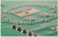
Figure 6: An example of fine pitch capability testing of jet printing with a 0.3-mm pitch BGA.
Figure 7: Beta test flow chart diagram.
Page 1 of 3


