


 Flexible Thinking: Designing Flex Circuits for Dynamic Reliability
 Global PCB Connections: Rigid-flex and Flexible PCBs—The Backbone of Modern Electronics
 Happy’s Tech Talk #29: Bend-to-Install Semi-flex FR-4


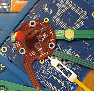
Laser Focus on Flex and Rigid-flex
January 28, 2019 | Barry Matties, I-Connect007Estimated reading time: 7 minutes
ESI’s Chris Ryder, director of Product Management, and Shane Noel, Flex Systems product manager, discuss laser vias for flex users and the increasing necessity for companies to collaborate early on and become more and more involved, whether that be in the product design, or with the process or base material manufacturers.
Barry Matties: First, can you start by telling us a little bit about ESI?
Chris Ryder: ESI is a company with a long tradition in electronics. The company has been around more than 70 years. In the last several decades, we’ve focused on laser-based processes. In particular, we are market leaders in using lasers for flex via drilling and other laser-based processes such as cutting, for example. While we’ve focused primarily on the UV laser regime, we’ve also recently made moves into other laser-based markets like HDI and ICP packaging. Of course, ESI has their foot in semiconductor manufacturing as well. We’re based in Portland, Oregon, but we have a global footprint. Most of our business stems from Asia; primarily China, Korea, Japan, and Taiwan.
Matties: When people design and integrate flex into their devices, what considerations do you think they should have with regard to manufacturing as it comes back into your area?
Shane Noel: The main thing that flex designers typically think about are traces, spaces, and via sizes. The incorporation of flex generally means you’re trying to conserve space, and conserving space requires you to design smaller vias, traces, and spaces. That drives the selection of materials. It’s typically based off polyimide and copper, although we see exotic material sets come into play more and more, especially with the advent of 5G technology. In general, you think of flexibility, of course. That’s important as well as reliability over the long term.
Matties: Do OEMs come to a process team like yours to talk about their flex designs, or do they just leave it up to the fabricator?
Ryder: That’s a good question. What we see is the necessity at this stage of the process for companies like ESI to be more and more involved in the product design. We also see a tighter requirement in terms of design rules between the material manufacturers, board designers, and process manufacturers. There’s a growing need for us to be involved in that discussion.
When you look at the link between the chipset, substrate, interposer, motherboard, and flex elements that go into that total construct, it becomes so dense that you have to imagine a room full of people packed so tightly that everybody has to talk about their intention to move around at every given point in time. That’s where we are in terms of the necessity to coordinate what we’re doing for the success of the actual device.
Matties: We’re talking also rigid-flex here, and you also mentioned the HDI. Are we starting to see HDI flex come to life?
Noel: I would say that’s a true statement. Rigid-flex had explosive growth last year and the year before. Traditionally, a lot of flex has been a connector between either two HDI boards or an HDI board and an antenna. Again, to reduce space consumption and allow for more functionality in a smaller device, you see this incorporation of the rigid and flex together.
Ryder: Chip-on-flex, for example. Instead of using a substrate-based fan-out for your chip, there are efforts to put the chip directly onto the flex in certain applications.
Matties: Where would an OEM go if they are looking to become a user of flex for the first time? What sort of advice would we give to them?
Noel: When we see customers enter the flex regime from either HDI or never having used flex, what they come to ESI for is the expertise on how to process the vias. Through-hole vias are simple; anybody can punch through a piece of material. Meanwhile, blind-hole vias are a little more of an art form. To maintain the reliability of your production floor and have low yield loss, you need to understand the process and understand the laser/material interaction. That’s really where ESI excels. We’ve been doing this for over 20 years and taken pains to understand what is going on when the laser meets the material.
Matties: From a designer’s point of view, you have to think differently.
Ryder: Yes. One of the challenges that we see is that you have material manufacturers with some materials that they’re bringing out for very specific applications such as high-frequency applications. The specifications or capabilities of the material, whether it’s electrical or structural reliability, can match the OEM’s expectation on paper and the data sheet. If you’re designing an antenna and need a certain dielectric constant, it all looks good on a data sheet. The reality is that manufacturing that part could bring some challenges.
Especially with the way we’re going right now towards 5G, we have a host of composite materials. When you add that element to the material (i.e., extra layers of materials with separate a Tg, Dk, filler content, etc.), it adds complication. It brings with it a challenge that you need to address if you really want to have high-yield, high-volume manufacturing. By getting involved with process manufacturers like ESI that do laser-based processes, you help yourself and guarantee the success of high yields, which everybody wants.
We’re a part of the puzzle. The material performances are key to the chipset of the antenna of any other function you have. Again, if you’re working with a subpar yield, it’s not going to help your product be successful. That’s the challenge we have, and that’s where I think the OEM would benefit by including us in the discussion.
Page 1 of 2
Share on:


Testimonial
"The I-Connect007 team is outstanding—kind, responsive, and a true marketing partner. Their design team created fresh, eye-catching ads, and their editorial support polished our content to let our brand shine. Thank you all! "
Sweeney Ng - CEE PCBSuggested Items
Nortech Systems Launches Power over Fiber Technology Platform for EMI-Sensitive Applications
04/08/2026 | Globe NewswireNortech Systems Incorporated, a leading provider of design and manufacturing solutions for complex electromedical devices and electromechanical systems, has announced the launch of its Power over Fiber technology platform.
Flexible Thinking: Designing Flex Circuits for Dynamic Reliability
04/09/2026 | Joe Fjelstad -- Column: Flexible ThinkingFlex circuits flex. No surprises there. However, they are also very commonly designed into products because they are thin and offer consistent thickness and dielectric properties, attributes highly prized by present-day product designers of personal electronics. This would include smartphones and, increasingly, wearable electronics for medical monitoring and even fashion.
Understanding Tolerances in Flexible Circuit Design
04/01/2026 | Chris Clark, Flexible Circuit TechnologiesThe challenge with cumulative tolerances is meeting the dimensional requirements for items dimensioned on a drawing or specification for a flexible or rigid-flex circuit. It is critical to understand the fabrication processes and how features are defined when creating your tolerance requirements.
Target Condition: An Exploration of Flooding PCB Layers
04/02/2026 | Kelly Dack -- Column: Target ConditionThe concept of flooding PCB layers with copper has been around for so long, you’d think we’d have it mastered. We haven’t. (Oh, and by “we,” I mean design engineers and the software tools we depend on.) Years ago, PCB artwork was created by hand using light tables, with tape applied to Mylar. Signals were slow, traces were relatively wide, and high-current paths were simply “beefed up” with wider copper. Signal integrity wasn’t yet a driving concern. Today, solid return paths are fundamental to robust design. We understand the importance of continuous reference planes for signal integrity and EMI control.
New, Greener Solutions for Etch: Novel Copper Extraction
03/30/2026 | Richard Nichols, GreenSource Engineering“Novel” is a typical marketing phrase that implies new and unique, but often “novel” actually means an established technology being applied to a new field or application. This, in turn, is often driven by newly relevant external motivation. GreenSource has been working on just such a solution: novel copper extraction, offering a better and greener alternative to traditional LLE control systems for cupric chloride etch.