-

-
News
News Highlights
- Books
Featured Books
- smt007 Magazine
Latest Issues
Current Issue
What's Your Sweet Spot?
Are you in a niche that’s growing or shrinking? Is it time to reassess and refocus? We spotlight companies thriving by redefining or reinforcing their niche. What are their insights?

Moving Forward With Confidence
In this issue, we focus on sales and quoting, workforce training, new IPC leadership in the U.S. and Canada, the effects of tariffs, CFX standards, and much more—all designed to provide perspective as you move through the cloud bank of today's shifting economic market.

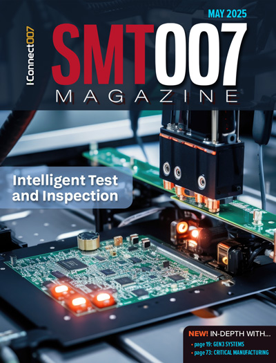
Intelligent Test and Inspection
Are you ready to explore the cutting-edge advancements shaping the electronics manufacturing industry? The May 2025 issue of SMT007 Magazine is packed with insights, innovations, and expert perspectives that you won’t want to miss.
- Articles
- Columns
- Links
- Media kit
||| MENU - smt007 Magazine
Impact of Stencil Foil Type on Solder Paste Transfer Efficiency for Laser-cut SMT Stencils (Part 1)
April 24, 2019 | Greg Smith, BlueRing StencilsEstimated reading time: 4 minutes
As innovation and demand continue to drive miniaturization in electronics, manufacturers face the constant challenge of assembling smaller and smaller components with repeatable processes and high yields. Stencil printing is the first step in the PWB assembly process, and improvements to the SMT stencil can significantly improve yields, especially for more challenging miniaturized products. The primary inputs in the SMT stencil manufacturing process are material, equipment, and processes, and by continuously improving these inputs, the overall print process is improved.
The most important material in the process of manufacturing SMT stencils is the foil itself. This article investigates foil types used with the goal of determining which foils provide the best print performance. The two foil alloys examined are stainless steel and electroformed nickel sheet, and each material will be measured with and without the application of ceramic nano-coatings. There have been many claims by stencil manufacturers in the industry over the past several years that fine grain foils cut and release solder paste better than other more standard stainless steel foils. However, the term "fine grain" has been used loosely and has not been well defined. Some users see print improvements using fine grain materials and some do not. This article correlates print performance to the grain size of each material tested and seeks to determine if the foil grain size is a primary factor in obtaining optimal print performance.
The term "print performance" is characterized by assessing transfer efficiency as well as print variation across a range of area ratios on both uncoated and ceramic nano-coated stencils for each material. SEM photographs are also presented, showing the surface topography of the sidewalls of the apertures after laser cutting. The SEM results are compared to the paste transfer efficiencies of each material to better understand how the aperture wall surface smoothness compares to SMT stencil performance. This study will show that the base foil used to manufacture SMT stencils does play an important role in overall stencil performance and is one of the most important inputs to provide the most consistent print process.
Experimental Methodology
A test vehicle was created that would show transfer efficiency over a wide array of area ratios. All seven materials are five mils thick (125 microns), and a rounded square was used to design each aperture. Each area ratio includes 100 apertures. The test vehicle is shown in Figure 1.
Figure 1: Test vehicle.
Two test vehicle patterns were laser cut into each stencil. One pattern on each stencil was coated with a ceramic nano-coating, and the other pattern was not coated. Two coupons were also cut into the top left and top right corners of each stencil. The coupons were outlined with a perforated pattern so that they could be removed and sent for SEM processing. The overall stencil image and coupon are shown in Figure 2.
Figure 2. Test stencil.
The coupon used for SEM photographs is also shown in Figure 3.
Figure 3: Test coupon.
The test coupon consists of two rows of apertures. Each row has one aperture of each size present in the test vehicle from 0.3 to 0.8. When cutting the coupons, each aperture was initially laser cut, and then a series of cuts were made across the midpoint of each aperture so that the coupon could be easily divided in half after being removed from the stencil. This allowed the SEM equipment to look directly into the sidewalls of the apertures. All stencils were cut on the same stencil on the same day with the same settings. The laser used was the most advanced stencil cutting laser currently in the market. One of the two patterns on each stencil was then coated with the same ceramic nano-coating equipment on the same day, and each was cured with the same parameters.
A 10-print study was run for each material type using a popular no-clean SAC305 Type 4 solder paste. The stencils were printed on bare copper clad material (0.062” or 1.57 mm) using an SMT carrier fixture holding two copper clad PWBs (Figure 4). This allowed both the uncoated and coated image to be printed at the same time minimizing as many variables as possible. The printer was a DEK Horizon 02i. Print parameters are shown in Table 1.
Figure 4: SMT carrier fixture.
Table 1: Solder paste printer parameters.
Solder paste volumes were measured using a 3D solder paste inspection system (SPI). The solder paste volume data was analyzed using statistical analysis software and the results were presented.
Seven different materials were evaluated and are listed in Table 2. Grain size is grouped into three categories. Category A includes stainless steel with grain sizes between 1–5 microns. Category B includes stainless steel with grain sizes between 6–10 microns, and Category C includes stainless steel with grain sizes over 10 microns. The grain size was not measured but was provided by the metal manufacturer. Category A is included in the “fine grain” category, and grain size was not available for the electroformed nickel material. For the purpose of this article, “fine grain” material is defined as material with a grain size of less than five microns.
Table 2: Materials tested.
Editor's Note: Stay tuned next week for the second part of this article, which will discuss the results of the experiment.
Suggested Items
Knocking Down the Bone Pile: Addressing End-of-life Component Solderability Issues, Part 4
07/15/2025 | Nash Bell -- Column: Knocking Down the Bone PileIn 1983, the Department of Defense identified that over 40% of military electronic system failures in the field were electrical, with approximately 50% attributed to poor solder connections. Investigations revealed that plated finishes, typically nickel or tin, were porous and non-intermetallic.
SHENMAO Strengthens Semiconductor Capabilities with Acquisition of PMTC
07/10/2025 | SHENMAOSHENMAO America, Inc. has announced the acquisition of Profound Material Technology Co., Ltd. (PMTC), a premier Taiwan-based manufacturer of high-performance solder balls for semiconductor packaging.
KYZEN to Highlight Understencil and PCB Cleaners at SMTA Querétaro Expo and Tech Forum
07/09/2025 | KYZEN'KYZEN, the global leader in innovative environmentally responsible cleaning chemistries, will exhibit at the SMTA Querétaro Expo & Tech Forum, scheduled to take place Thursday, July 24, at Centro de Congresos y Teatro Metropolitano de Querétaro.
Driving Innovation: Direct Imaging vs. Conventional Exposure
07/01/2025 | Simon Khesin -- Column: Driving InnovationMy first camera used Kodak film. I even experimented with developing photos in the bathroom, though I usually dropped the film off at a Kodak center and received the prints two weeks later, only to discover that some images were out of focus or poorly framed. Today, every smartphone contains a high-quality camera capable of producing stunning images instantly.
Hands-On Demos Now Available for Apollo Seiko’s EF and AF Selective Soldering Lines
06/30/2025 | Apollo SeikoApollo Seiko, a leading innovator in soldering technology, is excited to spotlight its expanded lineup of EF and AF Series Selective Soldering Systems, now available for live demonstrations in its newly dedicated demo room.


