


 The Right Approach: Get Ready for ISO 9001 Version 6
 Dan’s Biz Bookshelf: ‘Still Broke: Walmart’s Remarkable Transformation'
 Driving Innovation: Depth Routing Processes—Achieving Unparalleled Precision in Complex PCBs


Terahertz Technology Escapes the Cold
July 10, 2019 | ETH ZurichEstimated reading time: 5 minutes
Terahertz (THz) radiation is a bit like a treasure chest that resists being opened fully. Residing in the electromagnetic spectrum between the infrared and microwave regions, THz radiation combines a range of properties that are ideal with a view to applications. It provides a window to unique spectroscopic information about molecules and solids, it can penetrate non-conducting materials such as textiles and biological tissue, and it does so without ionising—and hence damaging—the object, or subject, under study. This opens up intriguing prospects for non-invasive imaging and non-destructive quality control, among other applications. But whereas there is no shortage in ideas for potential uses, their implementation is hampered by a lack of practical technologies for generating and detecting THz radiation.
Therefore the excitement as Lorenzo Bosco, Martin Franckié and colleagues from the group of Jérôme Faist at the Institute for Quantum Electronics of ETH Zurich reported now the realization of a THz quantum cascade laser that operates at a temperature of 210 K (-63 °C). That is the highest operational temperature achieved so far for this type of device. More importantly, this is the first time that operation of such a device has been demonstrated in a temperature regime where no cryogenic coolants are needed. Instead, Bosco et al. used a thermoelectric cooler, which is much more compact, cheaper and easier to maintain than cryogenic equipment. With this advance, they removed the main obstacles on the route to various practical applications.
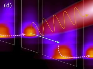
a) The thermoelectrically cooled laser box with the laser mounted on top of a Peltier element (white square), allowing operation between 195 K and 210.5 K with the laser emitting vertically through the window in the top lid. b) The laser chip as mounted in the laser box, contacted with thin gold wires bonded on top of several laser ridges. c) Schematic of one laser ridge; the horizontal lines show the quantum-well structure formed by layered semiconductors. The ridge (150 micrometres wide) is sandwiched between thin layers of copper. d) Conduction band edge (white lines) tilted by the applied operation bias, with the electron density resolved in energy shown in colour. The electrical bias drives electrons through the non-radiative transitions indicated by the dashed arrow. This pumps the state in the thin well, which becomes more populated than the state in the wider well indicated by the green arrow, allowing for net stimulated emission of terahertz photons.
A Cascade Towards Applications
Quantum cascade lasers (QCLs) have long been established as a natural concept for THz devices. Like many lasers that are widely used as sources of light in the visible-to-infrared frequency region, QCLs are based on semiconductor materials. But compared to typical semiconductor lasers used, for instance, in barcode readers or laser pointers, QCLs operate according to a fundamentally different concept to achieve light emission. In short, they are built around repeated stacks of precisely engineered semiconductor structures (see the figure, panel c), which are designed such that suitable electronic transitions take place in them (panel d). QCLs have been proposed in 1971, but they were first demonstrated only in 1994, by Faist and colleagues, then working at Bell Laboratories (US). The approach has proved its value in a board range of experiments, both fundamental and applied, mainly in the infrared region. The development of QCLs for THz emission has made substantial advances, too, starting from 2001. Widespread use has been hindered though by the requirement for cryogenic coolants -- typically liquid helium -- which adds substantial complexity and cost, and makes devices large and less mobile. Progress towards operation of THz QCLs at higher temperatures got essentially stuck seven years ago, when operation of devices at around 200 K (-73 °C) was achieved.
Page 1 of 2
Share on:


Testimonial
"We’re proud to call I-Connect007 a trusted partner. Their innovative approach and industry insight made our podcast collaboration a success by connecting us with the right audience and delivering real results."
Julia McCaffrey - NCAB GroupSuggested Items
Closing the Loop on PCB Etching Waste
09/09/2025 | Shawn Stone, IECAs the PCB industry continues its push toward greener, more cost-efficient operations, Sigma Engineering’s Mecer System offers a comprehensive solution to two of the industry’s most persistent pain points: etchant consumption and rinse water waste. Designed as a modular, fully automated platform, the Mecer System regenerates spent copper etchants—both alkaline and acidic—and simultaneously recycles rinse water, transforming a traditionally linear chemical process into a closed-loop system.
Driving Innovation: Depth Routing Processes—Achieving Unparalleled Precision in Complex PCBs
09/08/2025 | Kurt Palmer -- Column: Driving InnovationIn PCB manufacturing, the demand for increasingly complex and miniaturized designs continually pushes the boundaries of traditional fabrication methods, including depth routing. Success in these applications demands not only on robust machinery but also sophisticated control functions. PCB manufacturers rely on advanced machine features and process methodologies to meet their precise depth routing goals. Here, I’ll explore some crucial functions that empower manufacturers to master complex depth routing challenges.
Trouble in Your Tank: Minimizing Small-via Defects for High-reliability PCBs
08/27/2025 | Michael Carano -- Column: Trouble in Your TankTo quote the comedian Stephen Wright, “If at first you don’t succeed, then skydiving is not for you.” That can be the battle cry when you find that only small-diameter vias are exhibiting voids. Why are small holes more prone to voids than larger vias when processed through electroless copper? There are several reasons.
The Government Circuit: Navigating New Trade Headwinds and New Partnerships
08/25/2025 | Chris Mitchell -- Column: The Government CircuitAs global trade winds continue to howl, the electronics manufacturing industry finds itself at a critical juncture. After months of warnings, the U.S. Government has implemented a broad array of tariff increases, with fresh duties hitting copper-based products, semiconductors, and imports from many nations. On the positive side, tentative trade agreements with Europe, China, Japan, and other nations are providing at least some clarity and counterbalance.
How Good Design Enables Sustainable PCBs
08/21/2025 | Gerry Partida, Summit InterconnectSustainability has become a key focus for PCB companies seeking to reduce waste, conserve energy, and optimize resources. While many discussions on sustainability center around materials or energy-efficient processes, PCB design is an often overlooked factor that lies at the heart of manufacturing. Good design practices, especially those based on established IPC standards, play a central role in enabling sustainable PCB production. By ensuring designs are manufacturable and reliable, engineers can significantly reduce the environmental impact of their products.