


 Dan’s Biz Bookshelf: ‘Abundance: How We Build a Better Future’
 Trouble in Your Tank: In Complex Systems, Design Rules Aren’t Optional
 It’s Only Common Sense: The Phone Is Still Your Competitive Advantage


An Examination of Glass-fiber and Epoxy Interface Degradation in Printed Circuit Boards
July 12, 2019 | Bhanu Sood, Michael Osterman, and Michael Pecht, Center for Advanced Life Cycle EngineeringEstimated reading time: 7 minutes
Multilayer organic laminates, which make up over 90% of the interconnecting substrates in electronics (standard FR-4 represents 85% of the substrates used for laminates), can develop a loss of electrical insulation resistance between two biased conductors due to conductive filament formation. The probability of conductive filament formation is a function of the temperature, moisture content, voltage bias, manufacturing quality and processes, materials, and other environmental conditions and physical factors.
With increases in design density and tighter spacing between conductors, the probability of failure due to conductive filament formation (CFF) in printed circuit board (PCB) electronic assemblies has increased. CFF is a failure observed within glass-reinforced epoxy PCB laminates caused by an electrochemical process involving the ionic transport of a metal through or across a non-metallic medium under the influence of an applied electric field [1 & 2]. The growth of the metallic filament is a function of temperature, humidity, voltage, laminate materials, manufacturing processes, and the geometry and spacing of the conductors [2]. The growth of these filaments can cause an abrupt loss of insulation resistance between the conductors under a DC voltage bias.
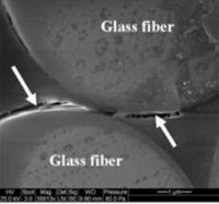
A statistical examination of field returns and root cause analysis performed at the Center for Advanced Life Cycle Engineering (CALCE) at the University of Maryland shows that failures in PCBs account for a significant percentage of field returns in electronic products and systems. Studies on CFF [2 & 3] have found that path formation in a PCB is often along the glass fiber to epoxy matrix interface (Figure 1).
Figure 1: Schematic describing CFF growth [3].
Delamination along the fiber-resin interface can occur as a result of stresses generated under thermal cycling due to coefficient of thermal expansion (CTE) mismatch between the glass fiber (CTE = ~5.5 ppm/°C) and the epoxy resin (CTE = ~65 ppm/°C) (Figure 2). CFF can take place in the plated through-hole to plated through-hole (PTH-PTH), PTH-plane, and trace-trace geometries.
Figure 2: CFF growth path along the glass fiber and resin interface [3].
A two-step model was developed to explain the growth of conductive filaments at the resin-glass interface in PCBs [1 & 3] where degradation of the resin-glass interfacial bond first occurs, followed by an electrochemical reaction. According to Lando [2], the path required for the transportation of metal ions formed by the degradation of the resin-glass interfacial bond results from the mechanical release of stresses, poor glass treatment, hydrolysis of the silane glass finish, or stresses originating from moisture-induced swelling of the epoxy resin.
Path formation was reported to be independent of bias; however, humidity was identified as a contributing factor towards degradation. After path formation, the PCB is viewed as an electrochemical cell. In this cell, the copper conductors are the electrodes, the absorbed water is the electrolyte, and the driving potential for the electrochemistry is the operating or test potential of the circuit. The electrode reactions for the metal migration are:
At the anode:
Equation 1:
Equation 2:
At the cathode:
Equation 3:
Pathway Formation in CFF
In PCBs, one manner in which the pathway between conductors is formed is through chemical hydrolysis of the silane glass finish or coupling agent. Past work has shown that the glass epoxy interface absorbs five to seven times more moisture than the bulk epoxy [5]. A common cross-linking agent used in FR-4 and many other epoxy-based laminated systems is dicyandiamide, or dicy. Dicy and glass surfaces are both hydrophilic. This combination of a hydrophilic surface and cross-linking agent is one of the factors responsible for the degradation of the glass fiber-epoxy resin interface due to hydrolysis. Williams [6] has shown that PCBs manufactured with non-dicy cross-linked epoxy resins are more resistance to CFF failures than PCBs manufactured with dicy cross-linked epoxy resins.
Organosilanes are bifunctional molecules that act as adhesion promoters, crosslink agents, and moisture scavengers in adhesive and sealant products [7]. Silane adhesion promoters act as molecular bridges between two chemically different materials and have been shown to dramatically improve the adhesion of polymeric resins to substrates such as glass, silica, alumina, or active metals.
Page 1 of 3
Share on:


Testimonial
"Advertising in PCB007 Magazine has been a great way to showcase our bare board testers to the right audience. The I-Connect007 team makes the process smooth and professional. We’re proud to be featured in such a trusted publication."
Klaus Koziol - atgSuggested Items
Driving Innovation: Selecting the Right Laser Source
04/28/2026 | Simon Khesin -- Column: Driving InnovationWhen I first joined Schmoll Maschinen, I brought experience from almost every PCB process, except for laser. As I immersed myself in laser processing, I realized why it can seem so daunting to a newcomer. The complexity arises from three intersecting factors: A vast variety of laser sources: CO2, UV-nano, green-pico, UV-pico, IR-pico, and others; a diverse range of applications: Drilling, cutting, ablation, and more; and an extensive list of materials: These have vastly different absorption rates. Choosing the right machine or laser source is rarely trivial. Even for experienced engineers, answering "Which source is best?" requires examining the business's specific goals.
Institute of Circuit Technology Spring Seminar 2026: A Bright Future in Europe
04/23/2026 | Pete Starkey, I-Connect007Through the leafy lanes and spring flowers of Warwickshire and back to Meridan, the traditional centre of England, and now officially part of the Metropolitan Borough of Solihull in the county of the West Midlands, I attended the Annual General Meeting and Spring Seminar of the Institute of Circuit Technology (ICT) on April 14. Out of the AGM came notable changes in leadership at the top of the Institute: the retirement of Mat Beadel as chair and Emma Hudson as technical director. Effective May 1, Steve Driver is the new chair, and Alun Morgan is the new technical director.
ACCM Unveils Negative and Near-zero CTE Materials for Large-Format AI Chips
04/21/2026 | Advanced Chip and Circuit MaterialsAdvanced Chip and Circuit Materials, Inc. (ACCM) has launched two new materials: Celeritas HM50, with a negative coefficient of thermal expansion (CTE) of -8 ppm/°C to offset the positive CTE and expansion of copper with temperature on circuit boards, and Celeritas HM001, with near-zero CTE and the low-loss performance needed for high-speed signal layers to 224 Gb/s and faster in artificial intelligence (AI) circuits.
Fresh PCB Concepts: Designing PCBs for Harsh Environments—Reliability Is Engineered Upstream
04/23/2026 | Team NCAB -- Column: Fresh PCB ConceptsWhen engineers hear the phrase “harsh environment,” they usually think of the extreme temperature swings, vibration and shock, pressure changes, or radiation in aerospace. However, aerospace is not the only harsh environment where electronic assemblies must survive. Automotive power electronics, downhole oil and gas tools, marine controls, rail systems, defense platforms, and industrial automation equipment all expose PCBs to environments that are equally unforgiving. The stress mechanisms may differ, but the physics does not.
Advanced Packaging for AI: Reliability Starts at the Cu/Cu/Cu Microvia Junction
04/20/2026 | Kuldip Johal, MKS' AtotechThe rapid growth of AI computing, from training clusters to inference at scale, is reshaping demand across the entire electronics supply chain. Advances in technology requirements, such as higher bandwidth, lower latency, and greater compute density, are driving the development of advanced packaging technologies and transforming the PCB industry across design, manufacturing, testing, and even architecture.