


 It’s Only Common Sense: The Importance of Setting Realistic Expectations
 Marcy’s Musings: The Relentless Pursuit of Perfection
 Dan’s Biz Bookshelf: ‘Do/Start'


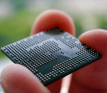
Optimizing Solder Paste Volume for Low-Temperature Reflow of BGA Packages
July 22, 2019 | Keith Sweatman, Nihon Superior Co. LtdEstimated reading time: 4 minutes
Abstract
The need to minimize thermal damage to components and laminates, reduce warpage-induced defects to BGA packages, and save energy is driving the electronics industry towards lower process temperatures. For soldering processes, the only way that temperatures can be substantially reduced is by using solders with lower melting points. Because of constraints of toxicity, cost, and performance, the number of alloys that can be used for electronics assembly is limited, and the best prospects appear to be those based around the eutectic in the Bi-Sn system, which has a melting point of about 139°C.
Experience so far indicates that such Bi-Sn alloys do not have the mechanical properties and microstructural stability necessary to deliver the reliability required for the mounting of BGA packages. Options for improving mechanical properties with alloying additions that do not also push the process temperature back over 200°C are limited. An alternative approach that maintains a low process temperature is to form a hybrid joint with a conventional solder ball reflowed with a Bi-Sn alloy paste. During reflow, there is mixing of the ball and paste alloys. But it has been found that to achieve the best reliability, a proportion of the ball alloy has to be retained in the joint, particularly in the part of the joint that is subjected to maximum shear stress in service—which is usually the area near component side. The challenge is then to find a reproducible method for controlling the fraction of the joint thickness that remains as the original solder ball alloy.
Empirical evidence indicates that, for a particular combination of ball and paste alloys and reflow temperature, the extent to which the ball alloy is consumed by mixing with the paste alloy depends on the volume of paste deposited on the pad. If this promising method of achieving lower process temperatures is to be implemented in mass production without compromising reliability, it would be necessary to have a method of ensuring the optimum proportion of ball alloy left in the joint after reflow can be consistently maintained.
In this article, the author explains how the volume of low-melting-point alloy paste that delivers the optimum proportion of retained ball alloy for a particular reflow temperature can be determined by reference to the phase diagrams of the ball and paste alloys. The example presented is based on the equilibrium phase diagram of the binary Bi-Sn system, but the method could be applied to any combination of ball and paste alloys for which at least a partial phase diagram is available or could be easily determined.
Introduction
The dependence of the electronics industry on solder to provide the reliable connections necessary to turn a collection of individual components into a functional circuit has created an ongoing dilemma that has challenged the industry since its inception. The main consideration in the design of electronic components is functionality; whether it be to provide a specific resistance, capacitance, or inductance in passive components; logical processing in integrated circuits; and responsiveness in sensors or just electrical connectivity. A need to survive the thermal profile required to form a joint with a molten metal has been an annoying complication.
The industry has had a fairly easy start with the Sn-Pb eutectic that has a relatively low melting point of 183°C and mechanical properties and microstructural stability that have been considered to be the benchmark for reliability in service. Because of the need to maximize heat transfer into the joint to get the substrates to wetting temperature, process temperatures (e.g., soldering tool tip temperature, wave solder bath temperature, reflow oven peak temperature) had to be substantially higher than that 183°C melting point. However, with proper process control, the temperature/time profile to which the most sensitive parts of the component were exposed could be kept within a safe limit.
The move to Pb-free solder brought a renewed challenge because the alloy endorsed by IPC as “the Pb-free alloy of choice for the electronics industry”—Sn-3.0Ag-0.5Cu (SAC305)—does not start to melt until 217°C, which is 34°C higher than the melting point of the Sn-37Pb it was replacing. However, as long as the higher process temperatures could be accommodated by the use of resins and polymers that could survive the higher thermal profiles, the electronics industry was able to adapt to this new alloy.
Figure 1: Defects caused by dynamic warpage of FCBGA components during reflow soldering.
When the problem with higher process temperatures was not just thermal degradation of materials but gross deformation of component packages the challenge moved to a new level. Integrated circuit packages have evolved into complex stacks of a wide range of materials with very different coefficients of thermal expansion so that as the package heats the differential expansion of bonded layers results in warpage of the package. The problem is exacerbated by the temperature gradients that develop within the package as a result of variations in thermal conductivity and thermal mass. The extent of warpage can mean that at its peak the warpage in area array packages is sufficient to cause complete separation of joints at their extreme edges (Figure 1).
Depending on the temperature at which that peak separation is reached for a particular component, the separation can take different forms:
1. Unreflowed solder paste can be split with some adhering to the solder ball and some to the pad
2. Unreflowed solder paste adheres only to the solder ball and is lifted off the pad
3. Unreflowed solder paste adheres only to the pad with the solder ball detaching from the solder paste
To read the full article, which appeared in the July 2019 issue of SMT007 Magazine, click here.
Share on:


Suggested Items
Koh Young Installs 24,000th Inspection System at Top 20 EMS
05/14/2025 | Koh YoungKoh Young, the global leader in True 3D measurement-based inspection and metrology solutions, proudly announces the installation of its 24,000th inspection system at a Top 20 Global EMS in Thailand.
Indium’s Karthik Vijay to Present on Dual Alloy Solder Paste Systems at SMTA’s Electronics in Harsh Environments Conference
05/06/2025 | Indium CorporationIndium Corporation Technical Manager, Europe, Africa, and the Middle East Karthik Vijay will deliver a technical presentation on dual alloy solder paste systems at SMTA’s Electronics in Harsh Environments Conference, May 20-22 in Amsterdam, Netherlands.
SolderKing Achieves the Prestigious King’s Award for Enterprise in International Trade
05/06/2025 | SolderKingSolderKing Assembly Materials Ltd, a leading British manufacturer of high-performance soldering materials and consumables, has been honoured with a King’s Award for Enterprise, one of the UK’s most respected business honours.
Knocking Down the Bone Pile: Gold Mitigation for Class 2 Electronics
05/07/2025 | Nash Bell -- Column: Knocking Down the Bone PileIn electronic assemblies, the integrity of connections between components is paramount for ensuring reliability and performance. Gold embrittlement and dissolution are two critical phenomena that can compromise this integrity. Gold embrittlement occurs when gold diffuses into solder joints or alloys, resulting in mechanical brittleness and an increased susceptibility to cracking. Conversely, gold dissolution involves the melting away of gold into solder or metal matrices, potentially altering the electrical and mechanical properties of the joint.
'Chill Out' with TopLine’s President Martin Hart to Discuss Cold Electronics at SPWG 2025
05/02/2025 | TopLineBraided Solder Columns can withstand the rigors of deep space cold and cryogenic environments, and represent a robust new solution to challenges facing next generation large packages in electronics assembly.