-

- News
- Books
Featured Books
- smt007 Magazine
Latest Issues
Current Issue
Spotlight on Mexico
Mexico isn’t just part of the electronics manufacturing conversation—it’s leading it. From growing investments to cross-border collaborations, Mexico is fast becoming the center of electronics in North America. This issue includes bilingual content, with all feature articles available in both English and Spanish.

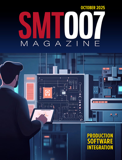
Production Software Integration
EMS companies need advanced software systems to thrive and compete. But these systems require significant effort to integrate and deploy. What is the reality, and how can we make it easier for everyone?

Spotlight on India
We invite you on a virtual tour of India’s thriving ecosystem, guided by the Global Electronics Association’s India office staff, who share their insights into the region’s growth and opportunities.
- Articles
Article Highlights
- Columns
- Links
- Media kit
||| MENU - smt007 Magazine
iNEMI Call for Participation Webinar Dec. 12
December 6, 2019 | iNEMIEstimated reading time: 1 minute
Flip chip electronic packages are commonly used to address today’s high-density interconnect needs. However, the formation of small voids (microvoids) can occur in solder-based flip chip joints during the assembly process and these voids tend to grow after multiple reflows. This can be a concern for certain applications that involve high electrical and thermal flux across the flip chip where void formation can have an impact on electromigration in the joint. The presence of a void can accelerate complete open failure due to electromigration.
This project will study voids in flip chip interconnect to determine their location and volume. It will also seek to understand how voiding in 1st level interconnect affects product reliability and what level of voiding is acceptable while maintaining reliability requirements. The project will have two distinct phases:
- Phase 1: Determine recommended inspection capabilities for micro-voids in 1st level interconnect materials
- Phase 2: Determine the relationship between voids and the electrical and mechanical reliability of the assembly
The project is expected to develop technical guidelines regarding acceptable voiding characteristics for flip chip interconnects that can be shared with industry and relevant standards bodies.
The 1st Level Interconnect Void Characterization Project is led by Lee Kor Oon (Intel) as project leader, with Sze Pei Lim (Indium) and Kiyoshi Ooi (Shinko) as co-leaders. Click here for additional project information.
Call-for-Participation Webinars
If you are interested in this project, please join us for one of our call-for-participation webinars. These webinars are open to industry (iNEMI membership is not required). Participants must register in advance. Click on the links below to register. For additional information, please contact Masahiro Tsuriya (m.tsuriya@inemi.org).
Session 1 (APAC)
Date: December 12, 2019
Time: 10:00 a.m. JST (Japan)
9:00 a.m. CST (China)
8:00 p.m. EST (U.S.) on Dec. 11
5:00 p.m. PST (U.S.) on Dec. 11
Session 2 (Americas and EMEA)
Date: December 12, 2019
Time: 7:00 a.m. EST (U.S.)
1:00 p.m. CET (Europe)
8:00 p.m. CST (China)
9:00 p.m. JST (Japan)
Testimonial
"Our marketing partnership with I-Connect007 is already delivering. Just a day after our press release went live, we received a direct inquiry about our updated products!"
Rachael Temple - AlltematedSuggested Items
BTU International Earns 2025 Step-by-Step Excellence Award for Its Aqua Scrub™ Flux Management System
10/29/2025 | BTU International, Inc.BTU International, Inc., a leading supplier of advanced thermal processing equipment for the electronics manufacturing market, has been recognized with a 2025 Step-by-Step Excellence Award (SbSEA) for its Aqua Scrub™ Flux Management Technology, featured on the company’s Pyramax™ and Aurora™ reflow ovens.
On the Line With… Ultra HDI Podcast—Episode 7: “Solder Mask: Beyond the Traces,” Now Available
10/31/2025 | I-Connect007I-Connect007 is excited to announce the release of the seventh episode of its 12-part podcast series, On the Line With… American Standard Circuits: Ultra HDI. In this episode, “Solder Mask: Beyond the Traces,” host Nolan Johnson sits down with John Johnson, Director of Quality and Advanced Technology at American Standard Circuits, to explore the essential role that solder mask plays in the Ultra HDI (UHDI) manufacturing process.
Rehm Wins Mexico Technology Award for CondensoXLine with Formic Acid
10/17/2025 | Rehm Thermal SystemsModern electronics manufacturing requires technologies with high reliability. By using formic acid in convection, condensation, and contact soldering, Rehm Thermal Systems’ equipment ensures reliable, void-free solder joints — even when using flux-free solder pastes.
Indium Experts to Deliver Technical Presentations at SMTA International
10/14/2025 | Indium CorporationAs one of the leading materials providers to the power electronics assembly industry, Indium Corporation experts will share their technical insight on a wide range of innovative solder solutions at SMTA International (SMTAI), to be held October 19-23 in Rosemont, Illinois.
Knocking Down the Bone Pile: Revamp Your Components with BGA Reballing
10/14/2025 | Nash Bell -- Column: Knocking Down the Bone PileBall grid array (BGA) components evolved from pin grid array (PGA) devices, carrying over many of the same electrical benefits while introducing a more compact and efficient interconnect format. Instead of discrete leads, BGAs rely on solder balls on the underside of the package to connect to the PCB. In some advanced designs, solder balls are on both the PCB and the BGA package. In stacked configurations, such as package-on-package (PoP), these solder balls also interconnect multiple packages, enabling higher functionality in a smaller footprint.


