


 It’s Only Common Sense: Marketing Isn’t Fluff, It’s Ammunition
 Driving Innovation: Mechanical and Optical Processes During Rigid-flex Production
 The Chemical Connection: Onshoring PCB Production—Daunting but Certainly Possible


Ventec Invests in Key Equipment to Support Expansion of PTFE Laminates Manufacturing
December 16, 2019 | Ventec International GroupEstimated reading time: 2 minutes
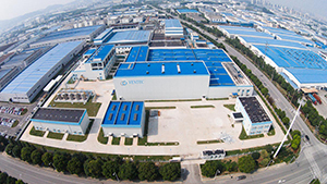
Ventec International Group Co., Ltd. has significantly increased its PTFE laminate manufacturing capabilities following a strategic investment in a new state-of-the-art high-temperature press and lay-up/break-down line at its Suzhou (China) manufacturing plant.
With 5G and evermore sophisticated radar applications, the demand and requirements for low loss/high frequency material is accelerating. Critical RF/Microwave-, antenna-, power amplifier- and sub-assembly-applications require superior electrical performance that can be delivered through PTFE laminates. To serve the increasing demand of these PTFE type products, Ventec has strengthened its investment in its Suzhou manufacturing plant to be even better positioned for the increase in demand and meet customers accelerated radar and 5G deployment requirements.
The most recent important equipment investment in a new state-of-the-art high-temperature press and lay-up/break-down line at Ventec’s Suzhou (China) manufacturing plant delivers a significant increase in manufacturing capacity to meet the growing demand for PTFE laminates. This includes the launch and roll-out of tec-speed 30.0 - Ventec’s latest ceramic filled high-speed/high-frequency PTFE material range that offers the highest signal-integrity characteristics for the most advanced high-frequency systems such as 77~79 GHz automotive radar systems.
tec-speed 30.0 (VT-3703) offers:
- Dk 3.0 with extremely low Df (0.0009)
- DK-stability versus temperature
- Lower in-plane thermal expansion
The current Dk 3.0 tec-speed 30.0 version will be supplemented by Dk 6.15 and Dk 10.2 versions in the first half of 2020, offering an even wider range of options for applications such as automotive radar, cellular base stations, power amplifiers & antennas, global positioning satellite antennas, patch antennas for wireless communication or power backplanes.
Jason Chung, CEO said: "The investment and installation of the PTFE manufacturing line is yet another important piece of the puzzle in our global growth program. The addition of the line to our range of capabilities demonstrates to our customers our commitment to maintaining the most up-to-date manufacturing technologies that support our clients’ PCB design, development and manufacturing needs."
For more information about Ventec's solutions and the company’s wide variety of products, please visit www.venteclaminates.com.
About Ventec International Group
Ventec International Group Co., Ltd. (6672 TT) is a premier supplier to the Global PCB industry. With volume manufacturing facilities in Taiwan and China and distribution locations and manufacturing sites in both the US and Europe, Ventec specializes in advanced copper clad glass reinforced and metal backed substrates. Ventec materials, which include high-quality enhanced FR4, high-speed/low-loss- & high-performance IMS material technology and an advanced range of thermal management solutions, are manufactured by Ventec using strict quality-controlled processes that are certified to AS9100 Revision D, IATF 16949:2016 and ISO 9001:2015, and are backed by a fully controlled and managed global supply chain, sales- and technical support-network.
Share on:


Testimonial
"We’re proud to call I-Connect007 a trusted partner. Their innovative approach and industry insight made our podcast collaboration a success by connecting us with the right audience and delivering real results."
Julia McCaffrey - NCAB GroupSuggested Items
WestDev Announces Advanced Thermal Analysis Integration for Pulsonix PCB Design Suite
10/29/2025 | WestDev Ltd.Pulsonix, the industry-leading PCB design software from WestDev Ltd., announced a major enhancement to its design ecosystem: a direct interface between Pulsonix and ADAM Research's TRM (Thermal Risk Management) analysis software.
Designers Notebook: Power and Ground Distribution Basics
10/29/2025 | Vern Solberg -- Column: Designer's NotebookThe principal objectives to be established during the planning stage are to define the interrelationship between all component elements and confirm that there is sufficient surface area for placement, the space needed to ensure efficient circuit interconnect, and to accommodate adequate power and ground distribution.
Episode 6 of Ultra HDI Podcast Series Explores Copper-filled Microvias in Advanced PCB Design and Fabrication
10/15/2025 | I-Connect007I-Connect007 has released Episode 6 of its acclaimed On the Line with... American Standard Circuits: Ultra High Density Interconnect (UHDI) podcast series. In this episode, “Copper Filling of Vias,” host Nolan Johnson once again welcomes John Johnson, Director of Quality and Advanced Technology at American Standard Circuits, for a deep dive into the pros and cons of copper plating microvias—from both the fabricator’s and designer’s perspectives.
Nolan’s Notes: Tariffs, Technologies, and Optimization
10/01/2025 | Nolan Johnson -- Column: Nolan's NotesLast month, SMT007 Magazine spotlighted India, and boy, did we pick a good time to do so. Tariff and trade news involving India was breaking like a storm surge. The U.S. tariffs shifted India from one of the most favorable trade agreements to the least favorable. Electronics continue to be exempt for the time being, but lest you think that we’re free and clear because we manufacture electronics, steel and aluminum are specifically called out at the 50% tariff levels.
MacDermid Alpha & Graphic PLC Lead UK’s First Horizontal Electroless Copper Installation
09/30/2025 | MacDermid Alpha & Graphic PLCMacDermid Alpha Electronics Solutions, a leading supplier of integrated materials and chemistries to the electronics industry, is proud to support Graphic PLC, a Somacis company, with the installation of the first horizontal electroless copper metallization process in the UK.